XG836 Datasheet
(Version 2.0: 2018-7-1)
��
6.3 Low Frequency Crystal Oscillator
14. Analog to Digital Converter��A/D��
15. Digital to Analog Converter��D/A��
16. Asynchronous Serial I/O -UART
17. Electrical Characteristics
17.2 Electrical Characteristics
XG836 is an 8-bit high performance, low cost MCU which bases on RISC architecture. It is easy to use to deal with analog signal, for example, measurement applications with sensor. The XG836 has an embedded 10-bit analog to digital converter (ADC) with 16 channels, two pulse width modulators (PWM) and one 8-bit digital to analog converter (DAC). It also improved some internal characteristics, such as Halt Function, Wake-up Function, Oscillator Selection, and Programmable Frequency Prescaler. So, XG836 is very flexible for use, and just need least extra parts for cutting down the cost. For these advantages and good characteristics, such as Integrated A/D, Integrated D/A, Integrated PWM, low cost, high performance, flexible Input/Output, and low price, XG836 is very suitable for applications such as Sensor signal process, Motor drive, Industry control, Consumed product, and subsystem controller etc.
XG836 uses Reduced Instruction Set, and it has 256 bytes RAM, the user can easily visit the ROM and RAM but no need to change program page. The special function registers have same addressing mode with RAM
XG836 is One-Time Programmable (OTP), and user��s program can be easily and effectively emulated by our emulator. It provides an effective way for users to develop their program.
�� High performance, low cost, 8-bit MCU
�� Advanced RISC architecture
- 59 instructions �C most of the instructions are executed within one single instruction cycle��Fosc/2��
�� Peripheral Features
- One 8-bit timer with frequency prescaler
- One 8-bit pulse width comparator with frequency prescaler
- Watch dog with independent oscillator
- One external interrupt
- One Timer with frequency prescaler and interrupt function.
- Embedded crystal and RC oscillator
- Program interfaces and code protection
- Low voltage reset��LVR��
- 15 I/O ports (P6��P7��P9��PA) with wake-up function
- Two channels of PWM
- 10-bit ADC with 15 channels
- 8-bit DAC with one channel
- A set of UART interface
- Two sets of SPI interface
�� Special Microcontroller Features
- Power on reset and power off detect
- Embedded, calibrated RC oscillator
- 6 hardware interrupt sources (external and internal)
- 8 levels stack
- Two sleep modes, halt and sleep to get low consumption
- Instructions are 16-bit��can visit all registers, RAM , ROM and no need to change program page
- Table read function
- Direct addressing and indirect addressing
- Bit oriented instructions
�� Memory
- 4K * 16bits OTP ROM
- 256 * 8bits RAM
- 128 * 8bits Special function registers
�� I/O and package
- 44 universal I/O ports
- There are two more inputs when use internal RC oscillator
�� Ambient operating temperature: 0 ~ 70��C
�� Operating voltage range: 2.3 ~ 5.5V
�� Operating Frequency range
1. Crystal mode: DC~20MHz at 5V, DC~8MHz at 3V,
2. RC oscillator mode: 3~20MHz at 5V, 3~8MHz at 3V,
�� Supply current of XG836 at 6MHz, 5V, 25��C
1. Normal Mode:
It depends on the level of the LDO,
when LDO=3volt, the operating current <1.5mA (no load and transition on all I/Os).
2. Sleep Mode:
< 4.5uA, when LDO on
< 1.5uA, when LDO off
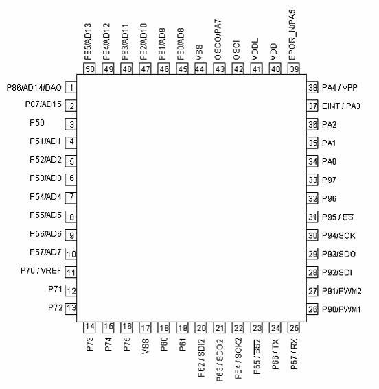
Figure 3.1 Pin assignment
Note: I = Input O = Output I/O = Input/Output P = Power
- = not use TTL = TTL Input ST = Schmitt Input
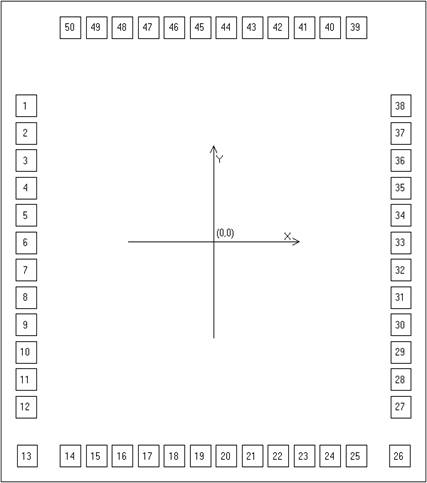
Figure 3.2 Pad Assignment
Unit:��m Note: the underlay must be connected to GND
|
NO. |
PAD NAME |
|
NO. |
PAD NAME |
|
1 |
P86/AD14/DAO |
26 |
P90/PWM1 |
|
|
2 |
P87/AD15 |
27 |
P91/PWM2 |
|
|
3 |
P50 |
28 |
P92/SDI |
|
|
4 |
P51/AD1 |
29 |
P93/SDO |
|
|
5 |
P52/AD2 |
30 |
P94/SCK |
|
|
6 |
P53/AD3 |
31 |
P95/SS |
|
|
7 |
P54/AD4 |
32 |
P96 |
|
|
8 |
P55/AD5 |
33 |
P97 |
|
|
9 |
P56/AD6 |
34 |
PA0 |
|
|
10 |
P57/AD7 |
35 |
PA1 |
|
|
11 |
P70/VREF |
36 |
PA2 |
|
|
12 |
P71 |
37 |
PA3/EINT |
|
|
13 |
P72 |
38 |
PA4/VPP |
|
|
14 |
P73 |
39 |
PA5/RESET |
|
|
15 |
CLK/P74/P76 |
40 |
VDD |
|
|
16 |
DATA/P75/P77 |
41 |
VDDL |
|
|
17 |
VSS |
42 |
OSCI |
|
|
18 |
P60 |
43 |
PA7/OSCO |
|
|
19 |
P61 |
44 |
VSS |
|
|
20 |
P62/SDI2 |
45 |
P80/AD8 |
|
|
21 |
P63/SDO2 |
46 |
P81/AD9 |
|
|
22 |
P64/SCK2 |
47 |
P82/AD10 |
|
|
23 |
P65/SS2 |
|
48 |
P83/AD11 |
|
24 |
P66/TX |
|
49 |
P84/AD12 |
|
25 |
P67/RX |
50 |
P85/AD13 |
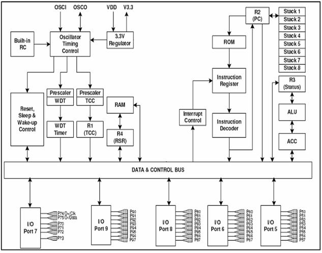
Figure 4.1 Functional Blocks
There are two main parts of memory space in XG836: Data memory and Program memory. And, XG836 has registers for special operation to those peripheral. Data memory have unified addresses with registers, but be separated from program memory.
XG836 has embedded 4K * 16bit OTP (One Time Programmable) ROM. The reset vector is 0XFFF, the hardware interrupt vector is 0X001, and software interrupt vector is 0X002.
XG836 has 256 * 8bits RAM as data memory, it has two addressing modes: Direct Addressing and Indirect Addressing through R0.
��
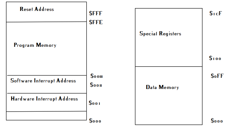
128 * 8bits special registers doesn��t have continuous addresses. The result is unknown to read or write to those undefined addresses.
Special registers can only be visited by direct addressing.
��
|
Name |
Address |
Bit7 |
Bit6 |
Bit5 |
Bit4 |
Bit3 |
Bit2 |
Bit1 |
Bit0 |
|
INDF |
100h |
Use content of FSR to address data memory��not a physical register.�� |
|||||||
|
TMR0 |
101h |
Timer0 register |
|||||||
|
PCL |
102h |
Low byte of Program counter��PC�� |
|||||||
|
STATUS |
103h |
GP |
|
|
T |
P |
Z |
DC |
C |
|
FSR |
104h |
Indirect data memory address pointer |
|||||||
|
P5 |
105h |
Data flip-latch of P5 when write, voltage status of P5 when read |
|||||||
|
P6 |
106h |
Data flip-latch of P6 when write, voltage status of P6 when read |
|||||||
|
P7 |
107h |
Data flip-latch of P7 when write, voltage status of P7 when read |
|||||||
|
P8 |
108h |
Data flip-latch of P8 when write, voltage status of P8 when read |
|||||||
|
P9 |
109h |
Data flip-latch of P9 when write, voltage status of P9 when read |
|||||||
|
IOC5 |
125h |
P5 I/O port control register |
|||||||
|
IOC6 |
126h |
P6 I/O port control register |
|||||||
|
IOC7 |
127h |
P7 I/O port control register |
|||||||
|
IOC8 |
128h |
P8 I/O port control register |
|||||||
|
IOC9 |
129h |
P9 I/O port control register |
|||||||
|
T1CON |
12Ch |
|
|
|
|
|
TM1E |
TM1P1 |
TM1P0 |
|
PULL_HIGH |
12Dh |
S7 |
|
/PUA |
/PU7 |
/PU9 |
/PU8 |
/PU6 |
/PU5 |
|
WDTCON |
12Eh |
|
ODE |
WDTE |
SLPC |
/WUEA |
/WUE9 |
/WUE7 |
/WUE |
|
INT_IE |
12Fh |
|
|
|
SPI2IE |
TM1IE |
SPIIE |
EXIE |
TCIE |
|
PWM1_DC |
130h |
PWM1 duty cycle register |
|||||||
|
PWM2_DC |
131h |
PWM2 duty cycle register |
|||||||
|
PWM1_PR |
132h |
PWM1 cycle register |
|||||||
|
PWM2_PR |
133h |
PWM2 cycle register |
|||||||
|
PWMCON |
134h |
PEN2 |
PEN1 |
PS2[2] |
PS2[1] |
PS[0] |
PS1[2] |
PS1[1] |
PS1[0] |
|
SPIRB |
13Ah |
SPI received data register |
|||||||
|
SPIWB |
13Bh |
SPI transmit data register |
|||||||
|
SPIS |
13Ch |
|
|
|
TM1IF |
OD3 |
OD4 |
RBFIF |
RBF |
|
SPIC |
13Dh |
CES |
SPIE |
SRO |
SSE |
ORD |
SBRS2 |
SBRS1 |
SBRS0 |
|
TMR1 |
13Eh |
Timer1 register |
|||||||
|
PWP |
13Fh |
Pulse width setup |
|||||||
��
��
��
��
��
��
��
��
��
��
��
��
��
��
��
��
��
��
��
��
��
��
��
��
��
��
��
��
��
��
��
��
��
��
��
|
Name |
Address |
Bit7 |
Bit6 |
Bit5 |
Bit4 |
Bit3 |
Bit2 |
Bit1 |
Bit0 |
|
ADCON |
140h |
ADC |
ADEN |
ACHEN |
|
CHS3 |
CHS2 |
CHS1 |
CHS0 |
|
AD_LSB |
141h |
AD1 |
AD0 |
|
|
|
|
|
|
|
AD_MSB |
142h |
AD9 |
AD8 |
AD7 |
AD6 |
AD5 |
AD4 |
AD3 |
AD2 |
|
ADCON2 |
143h |
VREF_IN |
|
|
|
|
ADPS2 |
ADPS1 |
ADPS0 |
|
PA |
148h |
Data flip-latch of PA when write, voltage status of PA when read |
|||||||
|
IOCA |
149h |
PA I/O port control register |
|||||||
|
PAL |
14Bh |
PA[6:0] |
PA_SEL |
||||||
|
PAH |
14Ch |
|
|
|
PA[11] |
PA[10] |
PA[9] |
PA[8] |
PA[7] |
|
DACON |
14Dh |
DA_EN |
|
RG2 |
RG1 |
RG0 |
|
|
|
|
DADAT |
14Eh |
DA7 |
DA6 |
DA5 |
DA4 |
DA3 |
DA2 |
DA1 |
DA0 |
|
UA_CON |
150h |
UA_EN |
RX_EN |
RX_IE |
|
BAUD16 |
TXF |
RXF |
RX_OV |
|
UA_BAUD |
151h |
BAUD7 |
BAUD6 |
BAUD5 |
BAUD4 |
BAUD3 |
BAUD2 |
BAUD1 |
BAUD0 |
|
UA_BUF |
152h |
UART data register |
|||||||
|
SPIRB2 |
15Ah |
SPI2 received data register |
|||||||
|
SPIWB2 |
15Bh |
SPI2 transmit data register |
|||||||
|
SPIS2 |
15Ch |
|
|
|
|
OD3 |
OD4 |
RBFIF |
RBF |
|
SPIC2 |
15Dh |
CES |
SPIE |
SRO |
SSE |
ORD |
SBRS2 |
SBRS1 |
SBRS0 |
|
ACHCON |
17Ah |
ACHEN7 |
ACHEN6 |
ACHEN5 |
ACHEN4 |
ACHEN3 |
ACHEN2 |
ACHEN1 |
|
|
GCKCON |
17Ch |
|
|
G_TMR1 |
G_ADC |
G_SPI2 |
G_SPI1 |
G_UART |
G_PWM |
|
R3F(INT_IF) |
17Fh |
|
|
|
SPI2IF |
TM1IF |
SPIIF |
EXIF |
TCIF |
Note: ��R: Readable, W: Writable, C: can be cleared
��RESE: Reset status
��U: Unchanged
A (Accumulator)
Internal data transfer, or instruction operand holding. It can��t be addressed.
INDF (Indirect address register) (Address: 0x100)
INDF is not a physical register. It is used for indirect addressing. Any instruction using R0 actually accesses the register pointed by FSR. While user reads data from INDF, the CPU gets data from the Data Memory at the address stored in FSR. While user writes the data into INDF, CPU actually saved the data into Data Memory at the address stored in FSR
TCC (Timer Register) (Address: 0x101)
This register is a 8-bit timer, can be read or written by program. It used to take count of internal clock. It has a programmable frequency prescaler��256 scale most��.
PCL (Program counter) and Stack (Address: 0x102)
R2 and hardware stack are 16 bits wide.
Generates 4096*16 on-chip ROM addresses to the relative programming instruction codes.
All bits of R2 are set to ��1�� as a RESET condition occurs.
• ��ADD R2, A�� allows relative address be loaded to current PC. Meanwhile, the high 8-bits of PC will be cleared.
•Any instruction that will change R2 (e.g. ��ADD R2, A��, ��MOV R2, A��, ��BC R2, 6�� etc, except ��TBL��), will cause the higher 8-bits of PC to be cleared. Thus, the computed jump is limited to the first 256 locations of any program page.
• ��TBL�� allows the relative address be loaded to current PC (R2 + A��R2), and the higher 8-bits of PC remains. Thus, the computed jump can be on any location of one program page.
• All instructions are executed within one instruction cycle(fclk/2) except for the instruction that would change the content of R2.
STATUS (Status Register) (Address: 0x103)
Status register contains the status of ALU calculation result and reset.
Just like the other registers, status register can be used as the destination operand of any instruction. If status register is used as destination operand, and the operation result affects either Z, DC, or C, then writing on Z, DC or C is prohibited. Setting or Clearing Z, DC, C depends on the logic module of the device.
Besides, T and P are un-writable. Thus, user may get an unexpected result if the status register is used as a destination operand.
Therefore if you want to change the content of the status register, we recommend you to use the bit oriented instructions (BC, BS), half-byte exchange instruction (SWAP), or move instruction (MOV R, A), because these instructions won��t affect Z, C, or DC.
|
Address |
7 |
6 |
5 |
4 |
3 |
2 |
1 |
0 |
|
0x103 |
GP |
- |
- |
T |
P |
Z |
DC |
C |
GP: General purpose read-write bit.
T: Time out flag
1: Power-on reset, SLEP instruction or WDTC instruction executed
0: A Watch Dog Timer time-out occurred
P: Power down flag
1: Power-on reset or WDTC instruction executed
0: SLEP instruction executed
Z: Zero flag
1: The result of arithmetic or Boolean calculation is zero
0: The result of arithmetic or Boolean calculation is not zero
DC: Digit carry/borrow flag��ADD��SUB instructions��
1: There is a carry out from the 4th bit of result
0: No carry out from the 4th bit of result
C: carry/borrow flag��ADD��SUB instructions��
1: There is a carry out from the most significant bit of result
0: No carry out from the most significant bit of result
Notes: The most or least significant bit of original register will be load to C after executing RLC and RRC instruction
FSR (RAM Select Register) (Address: 0x104)
Bits 0~7 , FSR is used for indirect addressing to select a register(address: 00~FF).
If the user doesn��t use indirect addressing, R4 can be used as a 8-bit general purpose read-write register.
P5 (Port 5 Register) (Address: 0x105)
|
|
Bit 7 |
Bit 6 |
Bit 5 |
Bit 4 |
Bit 3 |
Bit 2 |
Bit 1 |
Bit 0 |
|
Symbol |
P57/AD7 |
P56/AD6 |
P55/AD5 |
P54/AD4 |
P53/AD3 |
P52/AD2 |
P51/AD1 |
P50/AD0 |
|
R/W/C |
R/W |
R/W |
R/W |
R/W |
R/W |
R/W |
R/W |
R/W |
|
RESET |
0 |
0 |
0 |
0 |
0 |
0 |
0 |
0 |
While IOC5 is setup as input, and ACHEN=1 (in ADC_CON), CHS3~CHS0 are analog inputs, otherwise are general purpose I/O ports
P6 (Port 6 Register) (Address: 0x106)
|
|
Bit 7 |
Bit 6 |
Bit 5 |
Bit 4 |
Bit 3 |
Bit 2 |
Bit 1 |
Bit 0 |
|
Symbol |
P67/RX |
P66/TX |
P65/SS2 |
P64/SCK2 |
P63/SDO2 |
P62/SDI2 |
P61 |
P60 |
|
R/W/C |
R/W |
R/W |
R/W |
R/W |
R/W |
R/W |
R/W |
R/W |
|
RESET |
0 |
0 |
0 |
0 |
0 |
0 |
0 |
0 |
While SPI2 is enabled, P65-P62 are used for SPI function; While UART is enabled, P67-P66 are used as serial port, otherwise as general purpose I/O ports
P7 (Port 7 Register) (Address: 0x107)
|
|
Bit 7 |
Bit 6 |
Bit 5 |
Bit 4 |
Bit 3 |
Bit 2 |
Bit 1 |
Bit 0 |
|
Symbol |
P77 |
P76 |
P75/DATA |
P74/CLK |
P73 |
P72 |
P71 |
P70/VREF |
|
R/W/C |
R/W |
R/W |
R/W |
R/W |
R/W |
R/W |
R/W |
R/W |
|
RESET |
0 |
0 |
0 |
0 |
0 |
0 |
0 |
0 |
While ADC reference voltage input is enabled, P70 is ADC reference voltage input, the voltage must less than 3.6V, otherwise P70 is general purpose I/O port
P8 (Port 8 Register) (Address: 0x108)
|
|
Bit 7 |
Bit 6 |
Bit 5 |
Bit 4 |
Bit 3 |
Bit 2 |
Bit 1 |
Bit 0 |
|
Symbol |
P87/AD15 |
P86/AD14/DAO |
P85/AD13 |
P84/AD12 |
P83/AD11 |
P82/AD10 |
P81/AD9 |
P80/AD8 |
|
R/W/C |
R/W |
R/W |
R/W |
R/W |
R/W |
R/W |
R/W |
R/W |
|
RESET |
0 |
0 |
0 |
0 |
0 |
0 |
0 |
0 |
While IOC8 is setup as input, and ACHEN=1(in ADC_CON), CHS3~CHS0 are analog inputs; While DA is enabled, P86 is DA output, otherwise it is general purpose I/O port
P9 (Port 9 Register) (Address: 0x109)
|
|
Bit 7 |
Bit 6 |
Bit 5 |
Bit 4 |
Bit 3 |
Bit 2 |
Bit 1 |
Bit 0 |
|
Symbol |
P97 |
P96 |
P95/SS |
P94/SCK |
P93/SDO |
P92/SDI |
P91/PWM2 |
P90/PWM1 |
|
R/W/C |
R/W |
R/W |
R/W |
R/W |
R/W |
R/W |
R/W |
R/W |
|
RESET |
0 |
0 |
0 |
0 |
0 |
0 |
0 |
0 |
While SPI is enable, P95-P92 are used for SPI function; While PWM is enable, P91-P90 are used for PWM function, otherwise are general purpose I/O ports
CONTW (Write control register) (Address: 0x122)
CONTR (Read control register) (Address: 0x124)
CONTW is a writable register, and CONTR is a readable register, includes setup bit of TMR0 frequency prescaler and WDT frequency scaler(can be arranged register solely, called prescaler,too), and other control bits such as pull-high function of external interrupt and I/O ports
Ex.: To get 1:1 prescale for TMR0, the user can assign the prescaler to WDT.
|
|
Bit 7 |
Bit 6 |
Bit 5 |
Bit 4 |
Bit 3 |
Bit 2 |
Bit 1 |
Bit 0 |
|
Symbol |
/PHEN |
/INT |
|
|
PAB |
PSR2 |
PSR1 |
PSR0 |
|
R/W/C |
R/W |
R/W |
- |
- |
R/W |
R/W |
R/W |
R/W |
|
RESET |
1 |
0/U |
1 |
1 |
1 |
1 |
1 |
1 |
/PHEN: P6��P9 Pull-High Enable
1: Disable pull-high
0: Enable pull-high
/INT: Interrupt Enable
1: Enable interrupt by instruction ENI/RETI
0: Disable interrupt by instruction DISI
PAB: Prescaler Assign
1: Assign prescaler to WDT
0: Assign prescaler to Timer0
PSR2-0: TCC/WDT Prescaler setup
|
PSR2 |
PSR1 |
PSR0 |
TCC Rate |
WDT Rate |
|
0 |
0 |
0 |
1:2 |
1:1 |
|
0 |
0 |
1 |
1:4 |
1:2 |
|
0 |
1 |
0 |
1:8 |
1:4 |
|
0 |
1 |
1 |
1:16 |
1:8 |
|
1 |
0 |
0 |
1:32 |
1:16 |
|
1 |
0 |
1 |
1:64 |
1:32 |
|
1 |
1 |
0 |
1:128 |
1:64 |
|
1 |
1 |
1 |
1:256 |
1:128 |
IOC5 (P5 port control register) (Address: 0x125)
��1��: I/O is defined as input;
��0��: I/O is defined as output
IOC6 (P6 port control register) (Address: 0x126)
��1��: I/O is defined as input;
��0��: I/O is defined as output
IOC7 (P7 port control register) (Address: 0x127)
��1��: I/O is defined as input;
��0�� I/O is defined as output
IOC8 (P8 port control register) (Address: 0x128)
��1��: I/O is defined as input;
��0��: I/O is defined as output
IOC9 (P9 port control register) (Address: 0x129)
��1��: I/O is defined as input;
��0��: I/O is defined as output
IOC5, IOC6, IOC7, IOC8, IOC9, IOCA: all reset to 1
T1CON (Timer1 Control Register) (Address: 0x12C)
|
|
Bit 7 |
Bit 6 |
Bit 5 |
Bit 4 |
Bit 3 |
Bit 2 |
Bit 1 |
Bit 0 |
|
Symbol |
|
|
|
|
|
TM1E |
TM1P1 |
TM1P0 |
|
R/W/C |
|
|
|
|
|
R/W |
R/W |
R/W |
|
RESET |
|
|
|
|
|
0 |
0 |
0 |
TM1E: TIMER1 Enable
0: Disable timer1
1: Enable timer1
TM1P1-0: TIMER1 Frequency Prescaler Setup��prescale for Fosc/2��
|
TM1P1 |
TM1P0 |
Frequency scale |
|
0 |
0 |
1:1 |
|
0 |
1 |
1:4 |
|
1 |
0 |
1:8 |
|
1 |
1 |
1:16 |
PULL_HIGH (Pull High Control Register) (Address: 0x12D)
|
|
Bit 7 |
Bit 6 |
Bit 5 |
Bit 4 |
Bit 3 |
Bit 2 |
Bit 1 |
Bit 0 |
|
Symbol |
S7 |
|
/PUA |
/PU7 |
/PU9 |
/PU8 |
/PU6 |
/PU5 |
|
R/W/C |
R/W |
|
R/W |
R/W |
R/W |
R/W |
R/W |
R/W |
|
RESET |
1 |
|
1 |
1 |
1 |
1 |
1 |
1 |
Pull-high enable control.
0: Enable
1: Disable.
Port 6, port 9 pull-high is enabled or disabled by the result of /PU6��/PU9 AND with /PHEN
S7: Setup S7 to change the ability of sink current on P70-P73
1: Boost up the ability of sink current on P70-P73
0: P70-P73 has normal ability of sink current
/PUA: Setup the pull-low resisters of PA0-PA2 and pull-high resisters of PA3-PA5
1: Cut off the pull-low resisters of PA0-PA2 and pull-high resisters of PA3-PA5
0: Connect the pull-low resisters of PA0-PA2 and pull-high resisters of PA3-PA5
/PU7: Setup the internal pull-high resisters (2k) of P74 and P75
1: Cut off the internal pull-high resisters (2k) of P74 and P75
0: Connect the internal pull-high resisters (2k) of P74 and P75
/PU9: Setup the pull-high resisters of P9
1: Cut off the pull-high resisters of P9
0: Connect the pull-high resisters of P9
/PU8: Setup the pull-high resisters of P8
1: Cut off the pull-high resisters of P8
0: Connect the pull-high resisters of P8
/PU6: Setup the pull-high resisters of P6
1: Cut off the pull-high resisters of P6
0: Connect the pull-high resisters of P6
/PU5: Setup the pull-high resisters of P5
1: Cut off the pull-high resisters of P5
0: Connect the pull-high resisters of P5
WDTCON (WDT Control Register) (Address: 0x12E)
|
|
Bit 7 |
Bit 6 |
Bit 5 |
Bit 4 |
Bit 3 |
Bit 2 |
Bit 1 |
Bit 0 |
|
Symbol |
|
ODE |
WDTE |
SLPC |
/WUEA |
/WUE9 |
/WUE7 |
/WUE6 |
|
R/W/C |
|
R/W |
R/W |
R/W |
R/W |
R/W |
R/W |
R/W |
|
RESET |
|
0 |
1 |
1 |
1 |
1 |
1 |
1 |
ODE: Open-Drain Control
0: P76, P77 are general purpose I/O pins
1: P76, P77 are open drain outputs
WDTE: WDT Enable, only works while ENWDT =1 (in OPTION CODE)
0: WDT Disable
1: WDT Enable
WDT control. WDTE is invalid when ENWDT=0. It is said that while ENWDT=0,WDT can��t be enabled no matter what WDTE is. So WDTE is valid only while ENWDT=1. While ENWDT=1, WDT can be enable or disable by WDTE setup, 0=WDT enable�� 1=WDT disable. WDTE is a read-write bit.
SLPC: SLEEP2 mode control, clear this bit to enter SLEEP2 mode.
This bit can be set to be 1 by a wake-up signal produced by hardware, and can be cleared by software. SLPC is used to control oscillator, too. If it changes from high to low, the oscillator will stop (when oscillator stops, CPU enter SLEEP2 mode). If SLPC changes from low to high, the oscillator will start to work (CPU is waked up from SLEEP2 mode). To ensure the oscillator works stably, there is must a delay more than 18ms after waking up the oscillator. OST is activated while CPU is waked up from SLEEP2 mode, it will start to work no matter ENWDT=0 or 1. If ENWDT=1, WDT will be valid after waking up. SLPC is readable and writable.
/WUEA: Wake-Up by PA Enable
0: Wake up MCU by PA0~PA2 is allowed
1: Wake up MCU by PA0~PA2 is not allowed
/WUE9: Wake-Up by P9 Enable
0: Wake up MCU by P90~P92 is allowed
1: Wake up MCU by P90~P92 is not allowed
/WUE7: Wake-Up by P7 Enable
0: Wake up MCU by P74~P75 is allowed
1: Wake up MCU by P74~P75 is not allowed
/WUE6: Wake-Up by P6 Enable
0: Wake up MCU by P60~P67 is allowed
1: Wake up MCU by P60~P67 is not allowed
INTIE (Interrupt Enable Register) (Address: 0x12F)
INTIE is a readable and writable register. It contains enable bits for TMR0 time-out, external interrupt (INT)on falling edge, SPI and SPI2 interrupts, and TMR1 matching interrupt.
|
|
Bit 7 |
Bit 6 |
Bit 5 |
Bit 4 |
Bit 3 |
Bit 2 |
Bit 1 |
Bit 0 |
|
Symbol |
|
|
|
SPI2IE |
TM1IE |
SPIIE |
EXIE |
TCIE |
|
R/W/C |
|
|
|
R/W |
R/W |
R/W |
R/W |
R/W |
|
RESET |
|
|
|
0 |
0 |
0 |
0 |
0 |
SPI2IE: SPI2 Interrupt Enable
0: Disable SPI2 interrupt
1: Enable SPI2 interrupt
TM1IE: TIMER1 Interrupt Enable
0: Disable TIMER1 and PWP matching interrupt
1: Enable TIMER1 and PWP matching interrupt
SPIIE: SPI Interrupt Enable
0: Disable SPI interrupt
1: Enable SPI interrupt
EXIE: External Interrupt Enable
0: Disable external interrupt
1:Enable external interrupt
TCIE: TCC Interrupt Enable
0: Disable TCC time-out interrupt
1: Enable TCC time-out interrupt
PWM1_DC (PWM1 Duty Ratio Register) (Address: 0x130)
|
|
Bit 7 |
Bit 6 |
Bit 5 |
Bit 4 |
Bit 3 |
Bit 2 |
Bit 1 |
Bit 0 |
|
Symbol |
DAT7 |
DAT6 |
DAT5 |
DAT4 |
DAT3 |
DAT2 |
DAT1 |
DAT0 |
|
R/W/C |
R/W |
R/W |
R/W |
R/W |
R/W |
R/W |
R/W |
R/W |
|
RESET |
0 |
0 |
0 |
0 |
0 |
0 |
0 |
0 |

��
��
Duty Cycle = (PWM_DC/PWM_PR)*100��
PWM2_DC (PWM2 Duty Ratio Register) (Address: 0x131)
|
|
Bit 7 |
Bit 6 |
Bit 5 |
Bit 4 |
Bit 3 |
Bit 2 |
Bit 1 |
Bit 0 |
|
Symbol |
DAT7 |
DAT6 |
DAT5 |
DAT4 |
DAT3 |
DAT2 |
DAT1 |
DAT0 |
|
R/W/C |
R/W |
R/W |
R/W |
R/W |
R/W |
R/W |
R/W |
R/W |
|
RESET |
0 |
0 |
0 |
0 |
0 |
0 |
0 |
0 |
PWM1_PR (PWM1 Period Register) (Address: 0x132)
|
|
Bit 7 |
Bit 6 |
Bit 5 |
Bit 4 |
Bit 3 |
Bit 2 |
Bit 1 |
Bit 0 |
|
Symbol |
DAT7 |
DAT6 |
DAT5 |
DAT4 |
DAT3 |
DAT2 |
DAT1 |
DAT0 |
|
R/W/C |
R/W |
R/W |
R/W |
R/W |
R/W |
R/W |
R/W |
R/W |
|
RESET |
1 |
1 |
1 |
1 |
1 |
1 |
1 |
1 |
PWM2_PR (PWM2 Period Register) (Address: 0x133)
|
|
Bit 7 |
Bit 6 |
Bit 5 |
Bit 4 |
Bit 3 |
Bit 2 |
Bit 1 |
Bit 0 |
|
Symbol |
DAT7 |
DAT6 |
DAT5 |
DAT4 |
DAT3 |
DAT2 |
DAT1 |
DAT0 |
|
R/W/C |
R/W |
R/W |
R/W |
R/W |
R/W |
R/W |
R/W |
R/W |
|
RESET |
1 |
1 |
1 |
1 |
1 |
1 |
1 |
1 |
PWMCON (PWM Control Register) (Address: 0x134)
|
|
Bit 7 |
Bit 6 |
Bit 5 |
Bit 4 |
Bit 3 |
Bit 2 |
Bit 1 |
Bit 0 |
|
Symbol |
PEN2 |
PEN1 |
PS2[2] |
PS2[1] |
PS2[0] |
PS1[2] |
PS1[1] |
PS1[0] |
|
R/W/C |
R/W |
R/W |
R/W |
R/W |
R/W |
R/W |
R/W |
R/W |
|
RESET |
0 |
0 |
0 |
0 |
0 |
0 |
0 |
0 |
The three registers above are not readable, and instructions such as BS, BC, JBS, JBC are prohibited to use to them.
PE2-1: PWM1 and PWM2 control bit. PE2-1=1: PWM enable
PS2[2:0]/PS1[2:0] : PWM prescale
|
PS2 |
PS1 |
PS0 |
Clock��Hz�� |
Period |
|
0 |
0 |
0 |
Fosc/2 |
|
|
0 |
0 |
1 |
Fosc/4 |
|
|
0 |
1 |
0 |
Fosc/8 |
|
|
0 |
1 |
1 |
Fosc/16 |
|
|
1 |
0 |
0 |
Fosc/32 |
|
|
1 |
0 |
1 |
Fosc/64 |
|
|
1 |
1 |
0 |
Fosc/128 |
|
|
1 |
1 |
1 |
Fosc/256 |
|
PWM calculation:
PWM frequency = (Oscillation Frequency / PWM Clock / PWMI_PR
Duty Ratio = (PWMI_DC / PWMI_PR) * 100%
Example: Oscillation Frequency = 455 KHz PS2 [2:0] (Prescale) = 000 (clock = Fosc/2)
PWMI_PR = 6 PWMI_DC = 2
PWM frequency = 455K / 2 / 6 = 37.9 KHz
Duty Ratio = 2 / 6 * 100% = 33.3%
SPIRB (SPI Read Buffer) (Address: 0x13A)
|
|
Bit 7 |
Bit 6 |
Bit 5 |
Bit 4 |
Bit 3 |
Bit 2 |
Bit 1 |
Bit 0 |
|
Symbol |
DAT7 |
DAT6 |
DAT5 |
DAT4 |
DAT3 |
DAT2 |
DAT1 |
DAT0 |
|
R/W/C |
R/W |
R/W |
R/W |
R/W |
R/W |
R/W |
R/W |
R/W |
|
RESET |
U |
U |
U |
U |
U |
U |
U |
U |
8-bit data received is put into read buffer.
SPIWB (SPI Write Buffer) (Address: 0x13B)
|
|
Bit 7 |
Bit 6 |
Bit 5 |
Bit 4 |
Bit 3 |
Bit 2 |
Bit 1 |
Bit 0 |
|
Symbol |
DAT7 |
DAT6 |
DAT5 |
DAT4 |
DAT3 |
DAT2 |
DAT1 |
DAT0 |
|
R/W/C |
R/W |
R/W |
R/W |
R/W |
R/W |
R/W |
R/W |
R/W |
|
RESET |
U |
U |
U |
U |
U |
U |
U |
U |
8-bit data to be transmitted is put into write buffer.
SPIS (SPI Status Register) (Address: 0x13C)
|
|
Bit 7 |
Bit 6 |
Bit 5 |
Bit 4 |
Bit 3 |
Bit 2 |
Bit 1 |
Bit 0 |
|
Symbol |
- |
- |
- |
TMR1IF |
OD3 |
OD4 |
RBFIF |
RBF |
|
R/W/C |
|
|
|
R/W |
R/W |
R/W |
R/W |
R/W |
|
RESET |
|
|
|
0 |
0 |
0 |
0 |
0 |
TIMR1IF: TIMER1 Interrupt Flag
1: TIMER1 interruption occurred
0: No TIMER1 interruption occurred
OD3: Open Drain Control
1: SDO is set as open drain output
0: SDO isn��t set as open drain output
OD4: Open Drain Control
1: SCK is set as open drain output
0: SCK isn��t set as open drain output
RBFIF: Read Buffer Full Interrupt Flag
1: Receiving completed, SPIB buffer is full, and interruption occurred
0: Receiving is not completed, SPIB buffer is empty
RBF: Receive Buffer Full Flag
1: Receiving completed, SPIB buffer is full
0: Receiving is not completed, SPIB buffer is empty
SPIC (SPI Control Register) (Address: 0x13D)
|
|
Bit 7 |
Bit 6 |
Bit 5 |
Bit 4 |
Bit 3 |
Bit 2 |
Bit 1 |
Bit 0 |
|
Symbol |
CES |
SPIE |
SRO |
SSE |
ORD |
SBRS2 |
SBRS1 |
SBRS0 |
|
R/W/C |
R/W |
R/W |
R/W |
R/W |
R/W |
R/W |
R/W |
R/W |
|
RESET |
0 |
0 |
0 |
0 |
0 |
0 |
0 |
0 |
CES: Clock Edge Selection
1: Shift-out data at falling edge, shift-in data at rising edge, and holding data while high level
0: Shift-out data at rising edge, shift-in data at falling edge, and holding data while low level
SPIE: SPI Enable
1: Enable SPI
0: Disable SPI
SRO: SPI Buffer Overflow Flag
1: Old data has not been read while new data is loading. Only valid in slave mode.
0: Old data has been read while new data is loading. Only valid in slave mode.
SSE: SPI Shift Enable.
Start to shift-out data when set to 1, clear by hardware after shifting
ORD: Data Transmit Order
1: Lower bit first
0: Higher bit first
SBRS2-0: SPI Baud Rate Selection
|
SBRS2 |
SBRS1 |
SBRS0 |
MODE |
Baud Rate |
|
0 |
0 |
0 |
Master |
Fosc/2 |
|
0 |
0 |
1 |
Master |
Fosc/4 |
|
0 |
1 |
0 |
Master |
Fosc/8 |
|
0 |
1 |
1 |
Master |
Fosc/16 |
|
1 |
0 |
0 |
Master |
Fosc/32 |
|
1 |
0 |
1 |
Slave |
/SS enable |
|
1 |
1 |
0 |
Slave |
/SS disable |
|
1 |
1 |
1 |
Master |
TMR1/2 |
TMR1(TIMER1 Register) (Address: 0x13E)
|
|
Bit 7 |
Bit 6 |
Bit 5 |
Bit 4 |
Bit 3 |
Bit 2 |
Bit 1 |
Bit 0 |
|
Symbol |
TMR17 |
TMR16 |
TMR15 |
TMR14 |
TMR13 |
TMR12 |
TMR11 |
TMR10 |
|
R/W/C |
R/W |
R/W |
R/W |
R/W |
R/W |
R/W |
R/W |
R/W |
|
RESET |
0 |
0 |
0 |
0 |
0 |
0 |
0 |
0 |
This register is TIMER1��s counter, and the value will restart from 00 when it is equal to PWP.
PWP (Pulse Width Preset Register) (Address: 0x13F)
|
|
Bit 7 |
Bit 6 |
Bit 5 |
Bit 4 |
Bit 3 |
Bit 2 |
Bit 1 |
Bit 0 |
|
Symbol |
PWP7 |
PWP6 |
PWP5 |
PWP4 |
PWP3 |
PWP2 |
PWP1 |
PWP0 |
|
R/W/C |
R/W |
R/W |
R/W |
R/W |
R/W |
R/W |
R/W |
R/W |
|
RESET |
1 |
1 |
1 |
1 |
1 |
1 |
1 |
1 |
The desired width of baud clock is written to PWP in advance.
ADCON (AD Control Register) (Address: 0x140)
|
|
Bit 7 |
Bit 6 |
Bit 5 |
Bit 4 |
Bit 3 |
Bit 2 |
Bit 1 |
Bit 0 |
|
Symbol |
ADC |
ADEN |
ACHEN |
|
CHS3 |
CHS2 |
CHS1 |
CHS0 |
|
R/W/C |
R/W |
R/W |
R/W |
|
R/W |
R/W |
R/W |
R/W |
|
RESET |
0 |
0 |
0 |
|
0 |
0 |
0 |
0 |
ADC: AD Convert Complete Flag
0: Clear by hardware after AD converting
1: Set to 1 by software to enable AD converting
ADEN: ADC Enable
0: Disable AD
1: Enable AD
ACHEN: Channel Input Enable
0: Disable CH8~CH15(P80~P87) channel input
1: Enable CH8~CH15(P80~P87) channel input
CHS3 CHS2 CHS1 CHS0 : Analog Channel Selection
0 0 0 0 : no use
0 0 0 1 : AD1��P51��
0 0 1 0 : AD2��P52��
0 0 1 1 : AD3��P53��
0 1 0 0 : AD4��P54��
0 1 0 1 : AD5��P55��
0 1 1 0 : AD6��P56��
0 1 1 1 : AD7��P57��
1 0 0 0 : AD8��P80��
1 0 0 1 : AD9��P81��
1 0 1 0 : AD10��P82��
1 0 1 1 : AD11��P83��
1 1 0 0 : AD12��P84��
1 1 0 1 : AD13��P85��
1 1 1 0 : AD14��P86��
1 1 1 1 : AD15��P87��
AD_LSB (Least Significant 2 Bits of AD) (Address: 0x141)
|
|
Bit 7 |
Bit 6 |
Bit 5 |
Bit 4 |
Bit 3 |
Bit 2 |
Bit 1 |
Bit 0 |
|
Symbol |
AD1 |
AD0 |
|
|
|
|
|
|
|
R/W/C |
R |
R |
|
|
|
|
|
|
|
RESET |
U |
U |
|
|
|
|
|
|
The Least Significant 2 Bits of AD result
AD_MSB (Most Significant 8 bits of AD) (Address: 0x142)
|
|
Bit 7 |
Bit 6 |
Bit 5 |
Bit 4 |
Bit 3 |
Bit 2 |
Bit 1 |
Bit 0 |
|
Symbol |
AD9 |
AD8 |
AD7 |
AD6 |
AD5 |
AD4 |
AD3 |
AD2 |
|
R/W/C |
R |
R |
R |
R |
R |
R |
R |
R |
|
RESET |
U |
U |
U |
U |
U |
U |
U |
U |
The Most Significant 8 Bits of AD result
ADCON2 (AD Control Register) (Address: 0x143)
|
|
Bit 7 |
Bit 6 |
Bit 5 |
Bit 4 |
Bit 3 |
Bit 2 |
Bit 1 |
Bit 0 |
|
Symbol |
VREF_IN |
|
|
|
|
ADPS2 |
ADPS1 |
ADPS0 |
|
R/W/C |
R/W |
|
|
|
|
R/W |
R/W |
R/W |
|
RESET |
0 |
|
|
|
|
0 |
0 |
0 |
VREF_IN: ADC Reference Voltage Selection
0: Use internal LDO as reference voltage
1: Use voltage on P70 as reference voltage, and it must be less than 3.6V
ADPS[2:0]: ADC Clock Selection
|
ADPS2-ADS0 |
Clock��Hz�� |
|
000 |
Fosc/4 |
|
001 |
Fosc/8 |
|
010 |
Fosc/12 |
|
011 |
Fosc/16 |
|
100 |
Fosc/20 |
|
101 |
Fosc/24 |
|
110 |
Fosc/28 |
|
111 |
Fosc/32 |
ACHCON (AD Channel Control Register) (Address:0x17A)
|
|
Bit 7 |
Bit 6 |
Bit 5 |
Bit 4 |
Bit 3 |
Bit 2 |
Bit 1 |
Bit 0 |
|
Symbol |
ACHEN7 |
ACHEN6 |
ACHEN5 |
ACHEN4 |
ACHEN3 |
ACHEN2 |
ACHEN1 |
|
|
R/W/C |
R/W |
R/W |
R/W |
R/W |
R/W |
R/W |
R/W |
R/W |
|
RESET |
0 |
0 |
0 |
0 |
0 |
0 |
0 |
0 |
|
WDT_out |
0 |
0 |
0 |
0 |
0 |
0 |
0 |
0 |
|
Wake_up |
U |
U |
U |
U |
U |
U |
U |
U |
ACHEN7��CH7 channel input
0��Disable CH7(P57) channel input
1��Enable CH7(P57) channel input
ACHEN6��CH6 channel input
0��Disable CH6(P56) channel input
1��Enable CH6(P56) channel input
ACHEN5��CH5 channel input
0��Disable CH5(P55) channel input
1��Enable CH5(P55) channel input
ACHEN4��CH4 channel input
0��Disable CH4(P54) channel input
1��Enable CH4(P54) channel input
ACHEN3��CH3 channel input
0��Disable CH3(P53) channel input
1��Enable CH3(P53) channel input
ACHEN2��CH2 channel input
0��Disable CH2(P52) channel input
1��Enable CH2(P52) channel input
ACHEN1��CH1 channel input
0��Disable CH1(P51) channel input
1��Enable CH1(P51) channel input
PA (Port A) (Address: 0x148)
One general purpose register for I/O
IOCA (I/O A Control Register) (Address: 0x149)
1: Set the I/O as input
0: Set the I/O as output
PAL (Low 8 bits of Table Pointer) (Address: 0x14B)
PAH (High 8 bits of Table Pointer) (Address: 0x14C)
This method for looking up table could be used with no limit in any place of program memory. The table pointer must be set in advance. Do as this: put the low 7 bits of table address into PAL[7:1] . PAL[0] is used to define the high or low byte of table, if PAL[0]=0, it is low byte, otherwise is high byte. Put the high 6 bits address into PAH[5:0] . Then the data in table can be read by ��MOVC�� instruction from the memory that addressed by [PAH, PAL]
Example:
CODE_TAB:
MOV PAL, A ; Move the offset into PAL
MOV A, @((CODE_TAB_DB << 1 )& 0X00FF) ;Get the low 7 bits of table pointer
; address, and put them into PAL[7:1]
ADD PAL, A ; Add with the offset, and put the result into PAL
MOV A, @(CODE_TAB_DB >> 7) ;Get high 6 bits of table pointer address
MOV PAH, A ; put into PAH
MOVC ;Read data
RET
CODE_TAB_DB: ; Low 8 bits data in front
DB 0X014, 0X00F ; K1, K2
DB 0X00B, 0X00C ; K3, K4
DB 0X00E, 0X016 ; K5, K6
DB 0X000, 0X001 ; K7, K8
DACON (DA Control Register) (Address: 0x14D)
|
|
Bit 7 |
Bit 6 |
Bit 5 |
Bit 4 |
Bit 3 |
Bit 2 |
Bit 1 |
Bit 0 |
|
Symbol |
DA_EN |
|
RG2 |
RG1 |
RG0 |
|
|
|
|
R/W/C |
R/W |
|
R/W |
R/W |
R/W |
|
|
|
|
RESET |
0 |
|
0 |
0 |
0 |
|
|
|
DA_EN: DA Module Enable
0: Disable DA
1: Enable DA
RG2��RG1��RG0: Current Output Control
0 0 0 : No current output
1 0 0 : Current gain is 1
1 0 1 : Current gain is 2
1 1 0 : Current gain is 3
1 1 1 : Current gain is 4
DADAT (DA Data Register) (Address: 0x14E)
|
|
Bit 7 |
Bit 6 |
Bit 5 |
Bit 4 |
Bit 3 |
Bit 2 |
Bit 1 |
Bit 0 |
|
Symbol |
DA7 |
DA6 |
DA5 |
DA4 |
DA3 |
DA2 |
DA1 |
DA0 |
|
R/W/C |
R/W |
R/W |
R/W |
R/W |
R/W |
R/W |
R/W |
R/W |
|
RESET |
0 |
0 |
0 |
0 |
0 |
0 |
0 |
0 |
DA output data
UA_CON (UART Control Register) (Address: 0x150)
|
|
Bit 7 |
Bit 6 |
Bit 5 |
Bit 4 |
Bit 3 |
Bit 2 |
Bit 1 |
Bit 0 |
|
Symbol |
UA_EN |
RX_EN |
RX_IE |
|
BAUD16 |
TXF |
RXF |
RX_OV |
|
R/W/C |
R/W |
R/W |
R/W |
|
R/W |
R |
R |
R/C |
|
RESET |
0 |
0 |
0 |
|
0 |
0 |
0 |
0 |
UA_EN: UART Module Enable
0: Disable UART
1: Enable UART
RX_EN: Receive Enable
0: Disable receive
1: Enable receive
RX_IE: Receiving completed Interrupt Enable
0: Disable receive interrupt
1: Enable receive interrupt
BAUD16: Baud rate prescale
0: Fosc/4
1: Fosc/16
TXF: UART Transmitting Completed Flag
0: Transmitting completed
1: Transmitting
RXF: UART Receiving Completed Flag
0: Receiving completed
1: Receiving
RX_OV: UART Receive Overflow
0: UART receive overflow flag should be cleared by software
1: Set to 1 by hardware when UART receive overflows
UA_BAUD (UART Baud rate Register) (Address: 0x151)
|
|
Bit 7 |
Bit 6 |
Bit 5 |
Bit 4 |
Bit 3 |
Bit 2 |
Bit 1 |
Bit 0 |
|
Symbol |
BAUD7 |
BAUD6 |
BAUD5 |
BAUD4 |
BAUD3 |
BAUD2 |
BAUD1 |
BAUD0 |
|
R/W/C |
R/W |
R/W |
R/W |
R/W |
R/W |
R/W |
R/W |
R/W |
|
RESET |
U |
U |
U |
U |
U |
U |
U |
U |
Calculation of baud rate:
While UA_CON.BAUD16=1, Baud rate = (Fosc/16) / (UA_BAUD +1)
While UA_CON.BAUD16=0, Baud rate = (Fosc/4) / (UA_BAUD +1)
Example:
If Fosc=22.1184MHz��Baud rate = 115200Hz
Then, UA_BAUD=(22.1184M/16)/115200-1=12=0x0c
UA_BUF (UART Buffer) (Address: 0x152)
|
|
Bit 7 |
Bit 6 |
Bit 5 |
Bit 4 |
Bit 3 |
Bit 2 |
Bit 1 |
Bit 0 |
|
Symbol |
BUF7 |
BUF6 |
BUF5 |
BUF4 |
BUF3 |
BUF2 |
BUF1 |
BUF0 |
|
R/W/C |
R/W |
R/W |
R/W |
R/W |
R/W |
R/W |
R/W |
R/W |
|
RESET |
U |
U |
U |
U |
U |
U |
U |
U |
UART transmit and receive buffer
SPIRB2 (SPI2 Read Buffer) (Address: 0x15A)
|
|
Bit 7 |
Bit 6 |
Bit 5 |
Bit 4 |
Bit 3 |
Bit 2 |
Bit 1 |
Bit 0 |
|
Symbol |
DAT7 |
DAT6 |
DAT5 |
DAT4 |
DAT3 |
DAT2 |
DAT1 |
DAT0 |
|
R/W/C |
R/W |
R/W |
R/W |
R/W |
R/W |
R/W |
R/W |
R/W |
|
RESET |
U |
U |
U |
U |
U |
U |
U |
U |
8-bit data in SPI2 read buffer
SPIWB2 (SPI2 Write Buffer) (Address: 0x15B)
|
|
Bit 7 |
Bit 6 |
Bit 5 |
Bit 4 |
Bit 3 |
Bit 2 |
Bit 1 |
Bit 0 |
|
Symbol |
DAT7 |
DAT6 |
DAT5 |
DAT4 |
DAT3 |
DAT2 |
DAT1 |
DAT0 |
|
R/W/C |
R/W |
R/W |
R/W |
R/W |
R/W |
R/W |
R/W |
R/W |
|
RESET |
U |
U |
U |
U |
U |
U |
U |
U |
8-bit data in SPI2 write buffer
SPIS2 (SPI2 Status Register) (Address: 0x15C)
|
|
Bit 7 |
Bit 6 |
Bit 5 |
Bit 4 |
Bit 3 |
Bit 2 |
Bit 1 |
Bit 0 |
|
Symbol |
- |
- |
- |
|
OD3 |
OD4 |
RBFIF |
RBF |
|
R/W/C |
|
|
|
|
R/W |
R/W |
R/W |
R/W |
|
RESET |
|
|
|
|
0 |
0 |
0 |
0 |
OD3: Open Drain Control
1: SDO is set as open drain output
0: SDO isn��t set as open drain output
OD4: Open Drain Control
1: SCK is set as open drain output
0: SCK isn��t set as open drain output
RBFIF: Read Buffer Full Interrupt Flag
1: Receiving completed, SPIB buffer is full, and interruption occurred
0: Receiving is not completed, SPIB buffer is empty
RBF: Receive Buffer Full Flag
1: Receiving completed, SPIB buffer is full
0: Receiving is not completed, SPIB buffer is empty
SPIC2 (SPI2 Control Register) (Address: 0x15D)
|
|
Bit 7 |
Bit 6 |
Bit 5 |
Bit 4 |
Bit 3 |
Bit 2 |
Bit 1 |
Bit 0 |
|
Symbol |
CES |
SPIE |
SRO |
SSE |
ORD |
SBRS2 |
SBRS1 |
SBRS0 |
|
R/W/C |
R/W |
R/W |
R/W |
R/W |
R/W |
R/W |
R/W |
R/W |
|
RESET |
0 |
0 |
0 |
0 |
0 |
0 |
0 |
0 |
CES: Clock Edge Selection
1: Shift-out data at falling edge, shift-in data at rising edge
0: Shift-out data at rising edge, shift-in data at falling edge
SPIE: SPI Enable
1: Enable SPI
0: Disable SPI
SRO: SPI Buffer Overflow Flag
1: Old data has not been read while new data is loading. Only valid in slave mode.
0: Old data has been read while new data is loading. Only valid in slave mode.
SSE: SPI Shift Enable.
Start to shift-out data when set to 1, clear by hardware after shifting
ORD: Data Transmit Order
1: Lower bit first
0: Higher bit first
SBRS2-0: SPI Baud Rate Selection
|
SBRS2 |
SBRS1 |
SBRS0 |
MODE |
Baud Rate |
|
0 |
0 |
0 |
Master |
Fosc/2 |
|
0 |
0 |
1 |
Master |
Fosc/4 |
|
0 |
1 |
0 |
Master |
Fosc/8 |
|
0 |
1 |
1 |
Master |
Fosc/16 |
|
1 |
0 |
0 |
Master |
Fosc/32 |
|
1 |
0 |
1 |
Slave |
/SS enable |
|
1 |
1 |
0 |
Slave |
/SS disable |
|
1 |
1 |
1 |
Master |
Fosc/64 |
GCKCON (Clock Control Register) (Address: 0x17C)
|
|
Bit 7 |
Bit 6 |
Bit 5 |
Bit 4 |
Bit 3 |
Bit 2 |
Bit 1 |
Bit 0 |
|
Symbol |
|
|
G_TMR1 |
G_ADC |
G_SPI2 |
G_SPI1 |
G_UART |
G_PWM |
|
R/W/C |
R/W |
R/W |
R/W |
R/W |
R/W |
R/W |
R/W |
R/W |
|
RESET |
0 |
0 |
0 |
0 |
0 |
0 |
0 |
0 |
G_TMR1: TMR1 Clock Control bit
1: Enable TMR1 clock
0: Disable TMR1 clock
G_ADC: ADC, DAC Clock Control bit
1: Enable ADC, DAC clock
0: Disable ADC, DAC clock
G_SPI2: SPI2 Clock Control bit
1: Enable SPI2 clock
0: Disable SPI2 clock
G_SPI1: SPI1 Clock Control bit
1: Enable SPI1 clock
0: Disable SPI1 clock
G_UART: UART Clock Control bit
1: Enable UART clock
0: Disable UART clock
G_PWM: PWM Clock Control bit
1: Enable PWM clock
0: Disable PWM clock
ISR (Interrupt Status Register) (Address: 0x17F)
|
|
Bit 7 |
Bit 6 |
Bit 5 |
Bit 4 |
Bit 3 |
Bit 2 |
Bit 1 |
Bit 0 |
|
Symbol |
|
|
|
SPI2IF |
TMP1IF |
SPIIF |
EXIF |
TCIF |
|
R/W/C |
|
|
|
R/W |
R/W |
R/W |
R/W |
R/W |
|
RESET |
|
|
|
0 |
0 |
0 |
0 |
0 |
The result of reading ISR is the value of IOCF logic OR with ISR.
SPI2IF: SPI2 Interrupt Flag
1: SPI2 interrupt occurred
0: No SPI2 interrupt occurred
TM1IF: TIMER1 Interrupt Flag
1: TIMER1 interrupt occurred
0: No TIMER1 interrupt occurred
SPIIF: SPI Interrupt Flag
1: SPI interrupt occurred
0: No SPI interrupt occurred
EXIF: External Interrupt Flag
1: External interrupt occurred
0: No external interrupt occurred
TCIF: TCC Interrupt Flag
1: TCC interrupt occurred
0: No TCC interrupt occurred
XG836 can work in six different oscillator modes, and user can select one of them by configuring the oscillator selection:
1��LP Low speed, low cost crystal oscillator mode
2��HS High speed crystal oscillator/ceramic resonator
3��IRC Internal RC oscillator mode, PA7 output Fosc/2,
In most conditions, Pin OSCI and OSCO are connected to the crystal oscillator or ceramic resonator. The table below shows recommended values of C1, C2. Because of the difference between oscillators, user should select proper C1 and C2 according to the oscillator��s specification. And for low frequency application or in AT mode, there must be a resistor in series.
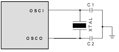
Figure 6.1: Circuit for Oscillator/Resonant (Parallel Mode)
Table: Capacitance Selection
|
Oscillator Type |
Frequency Mode |
Frequency |
C1(pF) |
C2(pF) |
|
Ceramic Resonator |
HXT |
455KHz |
10~150 |
10~150 |
|
1.0MHz |
40~80 |
40~80 |
||
|
2.0MHz |
20~40 |
20~40 |
||
|
4.0MHz |
10~30 |
10~30 |
||
|
Crystal Oscillator |
LXT |
32.768KHz |
25 |
15 |
|
100KHz |
25 |
25 |
||
|
200KHz |
25 |
25 |
||
|
HXT |
455KHz |
20~40 |
20~150 |
|
|
1.0MHz |
15~30 |
15~30 |
||
|
2.0MHz |
15 |
15 |
||
|
4.0MHz |
15 |
15 |
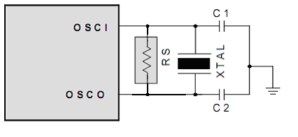
Figure 6.2: Circuit for Oscillator/Resonator (Resistance in Parallel)
For some applications that do not need a very precise timing calculation, the RC oscillator (as Figure 6.3) offers a lot of cost savings. Nevertheless, it should be noted that the frequency of the RC oscillator is influenced by the supply voltage, the values of the resistor (Rext), the capacitor (Cext), and even by the operation temperature. Moreover, the frequency also changes slightly from one chip to another due to the manufacturing process variation.
In order to maintain a stable system frequency, the values of the Cext should be 500pF, and that the value of Rext should not be greater than 1 Mohm. If they cannot be kept in this range, the frequency is easily affected by noise, humidity, and leakage.
The smaller the Rext in RC oscillator, the faster the frequency will be. On the contrary, for very low Rext, for instance, 1K��, the oscillator becomes unstable because the NMOS cannot discharge the current of the capacitance correctly.
Based on the reasons above, it must be kept in mind that all of the supply voltage, the operation temperature, the components of the RC oscillator, the package types, the way the PCB is layout, will affect the system frequency.
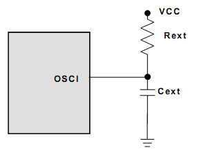
Figure 6.3: Circuit for External RC Oscillator
Notes: Cext = 500pF
|
Resistance |
Frequency |
Remark |
|
32��0x20�� |
20M |
|
|
70��0x46�� |
10M |
|
|
88��0x58�� |
8M |
|
|
118��0x76�� |
6M |
|
|
177��0xB1�� |
4M |
|
|
235��0xEB�� |
3M |
|
These relations between the resistance and frequency are just for reference. This option could be selected while programming. User can choose only the frequency which could be auto set by programmer; or choose resistance to get specific frequency.
XG836 can be driven by an external clock signal through the OSCI pin as shown in Figure below.
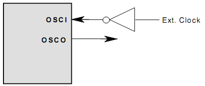
Figure 6.4: Circuit for External Clock Input
All I/O registers will be initialed after reset, and program will start from reset vector. The instruction at reset vector must be JMP to make sure that the program jumps to process resetting
If the source of reset is valid, it is not necessary that all clocks are normally running. After all reset signals disappear, a delay counter in chip will be activated to delay the reset process. For this, there is a certain time to let power supply reaching a stable level before MCU working.
Internal
resetting time = Power on resetting time + Oscillator starting up time
Power on resetting time: 18ms
Oscillator starting up time (OST) : 4.5ms / 9ms / 18ms /36ms / �� (by
option)
1. External reset. MCU will reset while the low level on RESET pin keeps longer than the Least Pulse Width.
2. Watchdog (if enabled) reset. Reset occurs while the watch dog is enabled and the watch dog timer is time-out.
3. Power off reset (if enabled). Reset occurs while the power-off detection is enabled and the voltage of power supply is less than the limit of power-off detection reset.
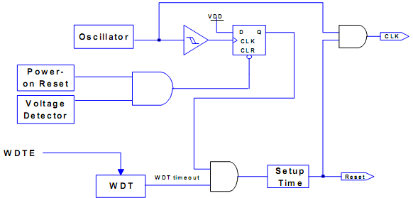
Figure 7.1: Reset Circuit Frame
The device is kept in a reset condition for a period of approx .18ms (oscillator starting up time) after reset occurs. Once reset occurs, the following functions will be performed.
? The oscillator is working, or will be started.
? All bits of the Program Counter (PCL) will be set to "1".
? While power is switched on, bits 5~6 of STATUS and the upper 2 bits of R4 will be cleared.
? All I/O port will be set as input (high-impedance state).
? The watchdog timer and prescaler will be cleared.
? The watchdog timer will be enabled if Code Option bit ENWDT is "1".
? Bits 3 and 6 of CONT register will be cleared, and bits 0, 4~5 of IOCE register will be set to ��1��.
? Bit 0 of R3F and bit 0 of IOCF will be cleared.
The sleep mode (power down) could be entered by executing SLEP instruction (named SLEEP1 MODE). While entering sleep mode, the WDT (if enabled) will be cleared but keep on running. The controller will be awakened by WDT overflow (if enabled), and go to reset. The T and P flags of R3 are used to judge the reset source (wake-up).
In addition to the basic SLEEP1 MODE, XG836 has another sleep mode(named SLEEP2 MODE), which is caused by clearing "SLPC" bit of IOCE register. In the SLEEP2 MODE, the controller can be awakened by following conditions:
(a) Any one of the wake-up pins is set to ��0��. Upon waking, the controller will continue to execute the program on-line. In this case, before entering SLEEP2 MODE, the wake-up function of the trigger sources (P60~P67) should be selected (e.g. input pin) and enabled (e.g. pull-high, wake-up control). One caution should be noted is that, after waking up, the WDT will be valid if Code Option bit ENWDT is "1". The operation to WDT (enable or disable) should be controlled by software after waking up.
(b) WDT overflows (if enabled). Once wake-up, it will cause the controller reset.
The XG836 has the following interrupts:
(1) TCC overflow interrupt
(2) External interrupt
(3) SPI interrupt
(4) Timer1 comparator match interrupt
(5) SPI2 interrupt
(6) UART receive interrupt
ISR (INTIF) is the interrupt status register, which records the interrupt request in flag bit. INTIE is the interrupt mask register. Global interrupt is enabled by ENI instruction and is disabled by DISI instruction. When one of the interrupts (if enabled) is generated, it will cause the next instruction to be fetched from address 001H. Once in the interrupt service routine, the source of the interrupt can be determined by polling the flag bits in the ISR register. The interrupt flag bit must be cleared by software before leaving the interrupt service routine, and enabling interrupts to avoid recursive interrupts. The flag in the Interrupt Status Register (ISR) is set regardless of the status of its mask bit or the execution of ENI instruction. Note that reading ISR will obtain the output of logic AND of ISR and INTIE. The RETI instruction exits interrupt routine and enables the global interrupt (execution of ENI instruction). When an interrupt is generated by INT instruction (if enabled), it causes the next instruction to be fetched from address 002H.
XG836 has three types of vector address: reset vector, hardware interrupt vector, software interrupt vector
Reset �� 0xfff
Hardware Interrupt �� 0x001
Software Interrupt �� 0x002
External interrupt is caused by EINT pin. User can enable the external interrupt function or disable it by setting EXIE bit of INTIE register. External interrupt can only be generated at falling edge.
Some I/O pins are multi-purpose; they could be general purpose I/O or pins for external function modules. Generally speaking, it can not be I/O pin while external function module is enabled.
The I/O registers, from Port 5 to Port A, are bi-directional tri-state I/O ports. P50~P57, P60~P67, P74~P75, P80~P87, P90~P97 and PA3~PA5 provide internal pull-high through software, and PA0~PA2 provides internal pull-low through software. P60~P67, P74~P75, P90~P91, and PA0~PA2 provide wake-up function through software. P76~P77 can have open-drain output by software control. P50~P57 and P80~P87 provide AD conversion function by software control, and P86 provide DA conversion function.
The I/O ports can be defined as "input" or "output" pins by the I/O control registers (IOC5~IOC9) under program control. The I/O registers and I/O control registers are both readable and writable. Note that the reading path source of input and output pins is different when reading the I/O port.
It is input when set I/O control register (IOC5~IOCA) to ��1��, and output when clear them to ��0��.
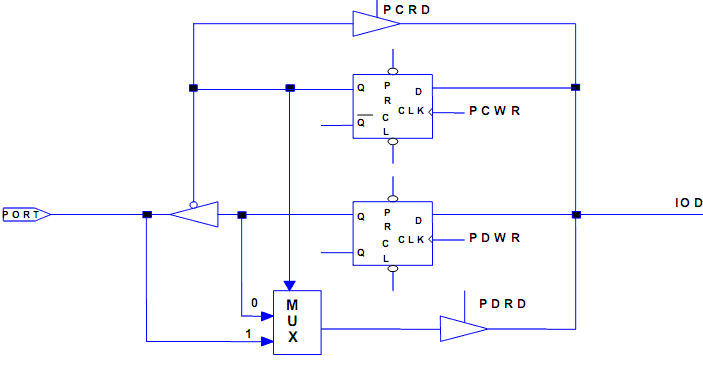
Figure 10.1: The Circuit of I/O Port and I/O Control Register
TIMER0 has the following characteristics:
? 8-bit timer
? Readable and writeable
? 8-bits programming prescaler
? Overflow interrupt occurs when counting from FFh to 00h
An 8-bit counter is available as prescaler for the TCC or WDT. The prescaler is available for either the TCC or WDT only at any given time, and the PAB bit of CONT register is used to determine the prescaler assignment. The prescaler is cleared each time by the instruction written to TCC under TCC mode. The WDT and prescaler, when assigned to WDT mode, are cleared by the WDTC or SLEP instructions.
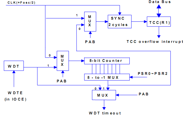
Figure 11.1: Block Diagram of TCC and WDT
TCC is an 8-bit timer/counter. TCC will increase by one at every instruction cycle (without prescaler).
WDT is a free running on-chip RC oscillator. The WDT will keep running even when the oscillator driver has been turned off (i.e. in sleep mode). During normal operation or sleep mode, a WDT time-out (if enabled) will cause the device to reset. The WDT can be enabled or disabled any time during the normal mode by software programming (if Code Option bit ENWDT is "1"). Refer to WDTE bit of IOCE register. Without prescaler, the WDT time-out period is approximately 18 ms.
The following Figure shows how XG836 communicates with other devices through SPI module. If XG836 is a master controller, it sends clock through the SCK pin. A couple of 8-bit data are transmitted and received at the same time. However, if XG836 is defined as a slave, its SCK pin could be programmed as an input pin. Data will continue to be shifted based on both the clock rate and the selected edge.
Features:
1) Operation in either Master mode or Slave mode
2) Three-wire or four-wire synchronous communication; that is, full duplex
3) Programmable baud rates of communication
4) Programmable clock polarity, (RD bit7)
5) Interrupt flag available for the read buffer full
6) Up to 8 MHz ( maximum ) bit frequency
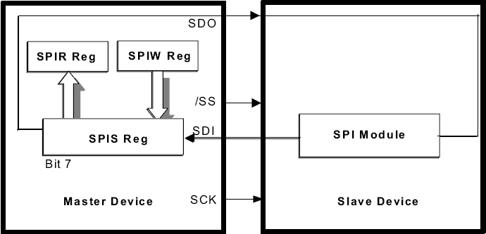
Figure 12.1: SPI Master/Slave Communication
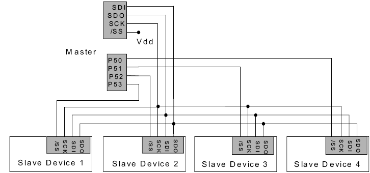
Figure 12.2: The SPI Configuration of Single-Master and Multi-Slave
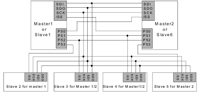
Figure 12.3: The SPI Configuration of Multi-Master and Multi-Slave
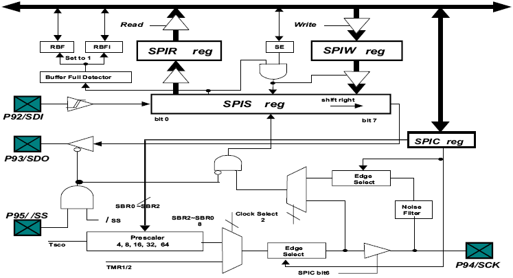
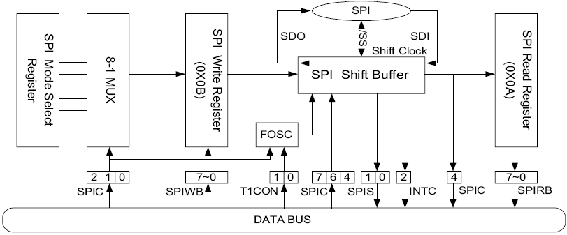
Figure 12.4: SPI Block Diagram
��
Figure 12.5: The Function Block Diagram of SPI Transmission
The following describes the function of each block and explains how to carry out the SPI communication:
• P92/SDI: Serial Data Input.
• P93/SDO: Serial Data Output.
• P94/SCK: Serial Clock.
• P95//SS: /Slave Selection(Option). This pin (/SS) may be required during a slave mode.
• RBF: Set to 1 by Buffer Full Detector, and cleared by software.
• RBIF: Set to 1 by Buffer Full Detector, and cleared by software (when interrupt enabled).
• Buffer Full Detector: Sets to 1 when an 8-bit shifting is completed.
• SSE: Loads the data into SPIS register, then start to shift
• SPIS register: Shifting byte in or out. The most significant bit is shifted first. Both the SPIS and SPIW registers are loaded at the same time. Once data is loaded, SPIS starts transmission or reception. The received data will be moved to the SPIR register when the shifting of the 8-bit data is completed. The RBF (Read Buffer Full) flag and the RBFI(Read Buffer Full Interrupt) flag are then set to 1.
• SPIR register: Read buffer. The buffer will not be written until the 8-bit shifting is completed.
• SBRS2~SBRS0: Program the clock frequency/rates and sources.
• Clock Select: Select either the internal or external clock as the shifting clock.
• Edge Select: Select the appropriate clock edges by programming the CES bit.
SPI Signal & Pin Description
The detailed functions of the eight pins, SDI (SDI2), SDO (SDO2), SCK (SCK2) and /SS (/SS2), are as below:
SDI/P92 (SDI2/P62):
• Serial Data In
• Receive serially
• Defined as high-impedance, if not selected
• Program the same clock rate and clock edge to latch on both the master and slave devices
• The new received byte will update the last received byte
• Both the RBF and RBFIF bits will be set to 1 as the SPI operation is completed
SDO/P93 (SDO2/P63):
• Serial Data Out
• Transmit serially
• Program the same clock rate and clock edge to latch on both the master and slave devices
• The new received byte will update the last received byte
• The CES bit will be cleared, as the SPI operation is completed
SCK/P94 (SCK2/P64):
• Serial Clock
• Generated by a master device
• Synchronize the data communication on both the SDI and SDO pins
• The CES is used to select the edge to communicate
• The SBR0~SBR2 is used to determine the baud rate of communication
• The CES and SBR0~SBR2 bits have no effect in the slave mode
/SS/P95 (/SS2/P65):
• Slave Select; negative logic
• Generated by a master device to signify the slave(s) to receive data
• Goes low before the first cycle of SCK appears, and remains low until the last (eighth) cycle is completed
• Ignores the data on the SDI and SDO pins while /SS is high, because the SDO is no longer driven
Timer1 (TMR1) is an 8-bit clock counter with a programmable prescaler. TMR1 can be read and written and cleared on any reset conditions. It can be turned down for power saving by clearing TMR1EN bit [T1CON<2>] to 0.
Figure 13.1 shows the TIMER1 block diagram. Each signal and block is described as follows:
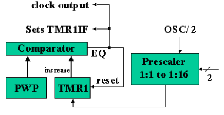
Figure 13.1: TIMER1 Block Diagram
• OSC/2: Input clock.
• Prescaler: Option of 1:1, 1:4, 1:8, and 1:16 defined by T1P1 and T1P02 (T1CON<1, 0>). It is cleared when a value is written to TMR1 or T1CON, and during any kind of reset as well.
• PWP: Pulse width preset register. The desired width of baud clock is written in advance.
• TMR1: Timer 1 register. TMR1 increases by 1 until it matches with PWP, and then resets to 0.
• Comparator: To change the output status while PWP and TMR1 matches. The TMR1IF flag will be set to 1 at the same time.
The Analog to Digital Converter��A/D��of XG836 has 16 analog channels
The A/D converter convert analog signal to 10-bitsdigital signal.
The A/D converter has a new characteristic that the sample rate is programmable. It allows user to select a new channel for converting, and set ADC immediately. After ADC is set, and before the converting actually starts, the selected channel has already begun to sample the signal according to the sampling rate set. It saves a lot of cost of hardware for sampling
There are 4 relative registers on this module:
- A/D Convert result register ( Higher byte)��AD_MSB��
- A/D Convert result register ( Lower byte)��AD_LSB��
- A/D Control register��ADCON��
- A/D Control register 2��ADCON2��
ADCON register is used to setup the function of A/D module pins, reference voltage, and enable AD converter. The ADCON2 register is used to setup the programmable sample rate
Any pin related to A/D converter can be set as analog input or digital I/O port.
AD_MSB and AD_LSB registers contain the result of A/D converting. When A/D converting completed, the result will be written into AD_MSB/AD_LSB registers, meanwhile the bit ADC (in ADCON register��will be cleared.
The value in AD_MSB:AD_LSB register remains the same during power-on reset. After power-on reset, the value in AD_MSB:AD_LSB register is uncertain. After the A/D converter module is set, and before the converting starts, the input channel for A/D convert must be selected. The IOC bit for the analog input channel must be set as input. If user wants to confirm the sampling period, please refer to ��Requirements for A/D sampling period��.
A/D setting is as following steps:
1. Set A/D convert module:
Select A/D input channels��ADCON��Bit 3~0��
Select A/D convert sample rate��ADCON2��Bit 2~0��
Best sample rate: 1M ~ 1.5M Hz
Enable clock of A/D module��GCKCON��Bit 4��
Enable A/D module and Analog Input Channel��ADCON��Bit 6��5)
2. Startup converting
Set ADC bit to ��1�� (ADCON, Bit 7)
3. Wait for A/D converting finish, judge as the following:
Test whether the status of ADC bit is 0.
4. Read the result from A/D result registers(AD_MSB: AD_LSB).
5. To the next A/D convert, go back to step1 or step2
The Digital to Analog Converter��D/A��of XG836 is 8-bit, and it has 256 levels. While DA_EN in DACON register is set to 1, the D/A module will start to convert the data in DADAT register to an analog signal (256 levels) , and the analog signal will be output by DAO pin. The output current can be changed according to the setup of RG2-RG0 in DACON register
Note: User should adjust the resistance of DAO according to the current
XG836 has a full-duplex serial I/O port which is easily used for communication with other chip that has such I/O port. UART function has an internal interrupt which is triggered when receiving dada or transmitting data finished.
UART Features
UART Functions:
Full-duplex asynchronism communication
8-bit Baud Rate Generator of Prescaler
UART external pins
UART communicates with other chip through TX and RX pins. UART function can be disabled by clearing UA_EN in UA_CON register, then TX and RX can be used as general purpose I/O ports. While UA_EN in UA_CON register is set to 1, the two I/O ports is used as TX output and RX input
Transmit Signal:
First, users should write the data to TXR register, then, under the control of baud rate generator, the data will be shifted to TX pin through transmit shift register bit by bit(lower bit first) . TXR has an address in data memory, so the program can visit it, but transmit shift register doesn��t have physical address, so it can��t be see in the user��s program.
Receiving Signal
Under the control of baud rate generator, data is shifted in by RX pin bit by bit( lower bit first) . When receiving completed, data will be moved from receive shift register to RXR register. Receive shift register doesn��t have physical address in data memory, so the program can��t visit it but RXR register
Actually, the registers TXR and RXR mentioned above share one address in data memory, it is UA_BUF register.
UART Status Control Register
There are three registers relate to UART function, they are UA_CON��UA_BAUD(control baud rate) and UA_BUF(a buffer used for transmit or receive data)
|
Items |
Rating |
|
Temperature under bias |
0��C to 70��C |
|
Storage temperature |
-20��C to 125��C |
|
DC Power supply |
2.3V to 5.5V |
|
Input voltage |
Vss-0.3V to VDD+0.3V |
|
Operating Frequency (2clk) |
DC to 12MHz |
AC Characteristics(TA=0�桫70��,VDD=3V & 5V)
|
Parameter |
Symbol |
Condition |
Min |
Typ |
Max |
Unit |
|
Input CLK duty cycle |
Dclk |
|
45 |
50 |
55 |
% |
|
Instruction cycle time (CLKS=��0��) |
Tins |
XTAL Type |
125 |
|
DC |
ns |
|
RC Type |
500 |
|
DC |
ns |
||
|
TCC input period |
Ttcc |
Note 1 |
(Tins+20)/N |
|
|
ns |
|
Input pin setup time |
Tset |
|
|
0 |
|
ns |
|
Input pin hold time |
Thold |
|
|
20 |
|
ns |
|
Output pin delay time |
Tdelay |
|
|
50 |
|
ns |
Note: N= Prescaler Coefficient
DC Characteristics(TA=0�桫70��,VDD=3V & 5V,LDO = 3.0V)
|
Parameter |
Testing Condition |
Min |
Typ |
Max |
Unit |
||
|
VDD |
Condition |
||||||
|
VDD |
Operating Voltage |
|
LDO on 3V fSYS=4MHz LVR disabled |
2.2 |
|
6.0 |
V |
|
LDO off fSYS=4MHz LVR disabled |
2.2 |
|
3.6 |
||||
|
Fxt |
Supply Oscillator Crystal |
3V |
One Cycle with two clocks
|
DC |
|
20 |
MHz |
|
5V |
DC |
|
20 |
||||
|
IIL1 |
Input Leakage Current for input pins |
3V |
VIN = VDD,VSS
|
|
|
1 |
uA |
|
5V |
|
|
1 |
||||
|
ICC1 |
Operating supply current |
2.4V |
Fosc = 32KHz,output pin floating, input pins at VDD, WDT disabled |
|
30 |
|
uA |
|
3V |
|
50 |
|
||||
|
ICC2 |
Operating supply current |
2.4V |
Fosc = 455KHz,output pin floating, input pins at VDD, WDT disabled |
|
150 |
|
uA |
|
3V |
|
200 |
|
||||
|
ICC3 |
Operating supply current |
2.4V |
Fosc = 4MHz,output pin floating, input pins at VDD, WDT disabled |
|
1.1 |
|
mA |
|
3V |
|
1.5 |
|
||||
|
ISTB1 |
Standby Current |
3V |
output pin floating, input pins at VDD, WDT disabled��LVR disabled |
|
1 |
|
UA |
|
5V |
|
1 |
|
||||
|
ISTB2 |
Standby Current |
3V |
output pin floating, input pins at VDD, WDT enabled��LVR disabled |
|
3 |
|
uA |
|
5V |
|
3 |
|
||||
|
ISTB3 |
Standby Current |
3V |
LDO = 2.4V, output pin floating, input pins at VDD, WDT disabled��LVR enabled |
|
2 |
|
uA |
|
5V |
|
3 |
|
||||
|
ISTB3 |
Standby Current |
3V |
LDO = 3V, output pin floating, input pins at VDD, WDT disabled��LVR enabled |
|
3 |
|
uA |
|
5V |
|
4 |
|
||||
|
ISTB4 |
Standby Current |
3V |
LDO = 2.4V, output pin floating, input pins at VDD, WDT enabled��LVR enabled |
|
3 |
|
uA |
|
5V |
|
3 |
|
||||
|
ISTB4 |
Standby Current |
3V |
LDO = 3V, output pin floating, input pins at VDD, WDT enabled��LVR enabled |
|
3 |
|
uA |
|
5V |
|
4 |
|
||||
|
IADC1 |
ADC Current |
3V |
LDO = off, P70 Current |
|
800 |
|
uA |
|
VIH1 |
Input High Voltage |
3V |
|
1.5 |
|
|
V |
|
5V |
2.5 |
|
|
||||
|
VIH2 |
Input High Voltage |
3V |
PA6,PA7 input |
1.2 |
|
3.0 |
V |
|
5V |
2.0 |
|
3.0 |
||||
|
VIL1 |
Input Low Voltage |
3V |
|
|
|
0.6 |
V |
|
5V |
|
|
1.0 |
||||
|
VIHX |
Clock Input High Voltage |
3V |
OSCI |
|
1.52 |
|
V |
|
5V |
|
1.76 |
|
||||
|
VILX |
Clock Input Low Voltage |
3V |
OSCI |
|
0.76 |
|
V |
|
5V |
|
1.0 |
|
||||
|
VOH1 |
Output High Voltage |
3V |
IOH = 8mA |
|
2.4 |
|
V |
|
5V |
|
4.4 |
|
||||
|
VOL1 |
Output Low Voltage |
3V |
IOL = 10mA |
|
0.4 |
|
V |
|
5V |
|
0.4 |
|
||||
|
VOL2 |
Output Low Voltage |
3V |
IOL = 20mA |
|
0.4 |
|
V |
|
5V |
|
0.4 |
|
||||
|
IPH |
Pull-high current |
3V |
Pull-high active, input pin at Vss |
|
30 |
|
uA |
|
5V |
|
100 |
|
||||
2018-07-01 XINGA.