1. summary
Xg628 single chip integrates USB, PD and other fast charging protocols, and supports PD3 0/2.0,BC1. Second class boost fast charging protocol, automatic detection
Vconn and analog E-MARK chip, up to 100W power, built-in PD communication module, high integration and simplified periphery. Integrated output voltage detection function, and provides over-temperature, over-voltage protection and other functions. It can be widely used in various electronic devices to expand high-power input, such as wireless charger, electric toothbrush, rechargeable razor, lithium battery power tools and other applications.
2. Functional features
Support 4V to 22V input voltage
Support PD3 0/2.0,BC1. Second class fast charging protocol
Support USB type-C PD, forward and reverse plug detection and automatic switching
Support E-MARK simulation, automatically detect vconn, and support PD request of 100W power
The request voltage can be dynamically adjusted in a variety of ways
High single-chip integration, simplified periphery and low cost
Built in overvoltage protection module ova and overtemperature protection module OTA
3. Application occasion
Wireless charger
Laptop charging cable
Lithium battery small household appliances
Lithium battery power tools
portable source
4. Pin Out
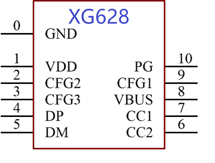
Xg628 package pin arrangement
|
Number
|
Pin Name
|
Type
|
Description
|
|
XG628
|
|
0
|
GND
|
power
|
Common ground terminal, heat dissipation base plate
|
|
1
|
VDD
|
power
|
Working power input, external 1uF decoupling capacitor, series resistance to VBUS
|
|
4,5
|
DP,DM
|
Two way
|
USB bus
|
|
6,7
|
CC1,CC2
|
Two way
|
Type-C CC bus
|
|
2,3,9
|
CFG1,CFG2,
CFG3
|
Analog input
|
Voltage configuration input
|
|
8
|
VBUS
|
Analog input
|
Voltage detection input requires series resistance to the external input VBUS
|
|
10
|
PG
|
Open drain output
|
Default Hi-Z, customizable function
|
5. Function description
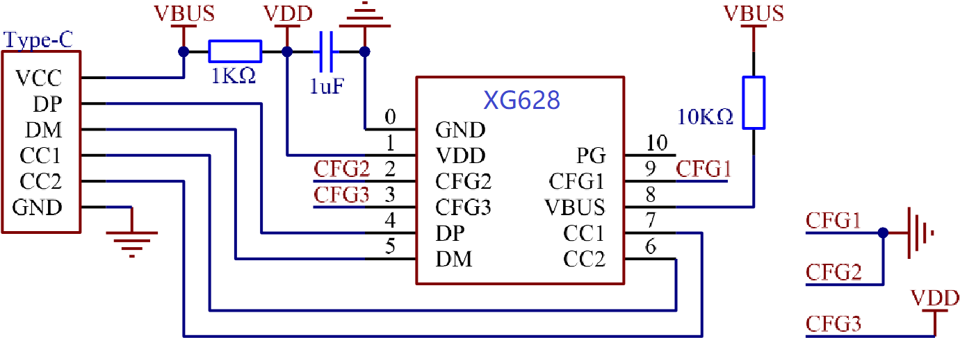
Xg628 is a PD3 0/2.0,BC1. The power receiving terminal IC of protocol power supply input by class 2 boost and fast charging protocol supports the request of voltage in the range of 4 ~ 22V, and can dynamically configure the voltage gear of priority request in a variety of ways.
Xg628 provides single resistance configuration mode and level configuration mode.
6. level configuration
It is suitable for MCU dynamic adjustment request voltage or PCB fixed request voltage.
Cfg1, CFG2 and cfg3 are directly connected to the IO port of the external MCU, or directly connected to the VDD / GND pin of xg628 chip, and the level is used to configure the request voltage. The truth table is as follows.
|
CFG1
|
CFG2
|
CFG3
|
Adjust voltage output
|
|
1
|
-
|
-
|
5V
|
|
0
|
0
|
0
|
9V
|
|
0
|
0
|
1
|
12V
|
|
0
|
1
|
1
|
15V
|
|
0
|
1
|
0
|
20V
|
When using the level configuration mode, pay attention to the selection of IO port mode and default state.
For xg628, the input voltage of cfg1 pin shall not be higher than 8V, and the input voltage of CFG2 / cfg3 pin shall not be higher than 3.7V. When cfg1 uses the IO input high level of open drain pull-up mode, if its pull-up resistance is large, it may be determined as a single resistance configuration by xg628. Therefore, if the push-pull mode cannot be used to drive cfg1, additional pull-up resistance shall be added to ensure the pull-up driving capacity.
If the back-end circuit such as MCU starts slowly, cfg1 may be in floating state and request 20V before starting. If the system cannot bear 20V input, configuration resistance should be added to cfg1 pin to ensure that xg628 can request appropriate voltage before starting the back-end circuit.
5.3. Xg628 uses type-C female port with level configuration of 5 / 9 / 12 / 15 / 20V
|
CFG1
|
CFG2
|
CFG3
|
Adjust voltage output
|
|
1
|
-
|
-
|
5V
|
|
0
|
0
|
0
|
9V
|
|
0
|
0
|
1
|
12V
|
|
0
|
1
|
1
|
15V
|
Parameters
7.1. Absolute maximum value (critical or exceeding the absolute maximum value may cause abnormal operation or even damage of the chip)
|
name
|
Parameter description
|
Minimum value
|
Maximum
value
|
unit
|
|
TA
|
Ambient temperature during operation
|
-40
|
90
|
℃
|
|
TS
|
Ambient temperature during storage
|
-55
|
105
|
℃
|
|
VDD
|
Working power supply voltage (VDD pin is connected to power supply, GND pin is connected to ground)
|
3.0
|
3.6
|
V
|
|
VIOHV
|
Supports the voltage on the high voltage pin (CFG, VBUS)
|
-0.5
|
13.5
|
V
|
|
VIOCC
|
Voltage on CC1, CC2, cfg1 pins
|
-0.5
|
8
|
V
|
|
VIOUX
|
Voltage on DP, DM, CFG, CFG2, cfg3 pins
|
-0.5
|
VDD+0.5
|
V
|
|
VIOLV
|
Voltage on cfghv pin
|
|
0.8
|
V
|
|
PD
|
Maximum power consumption of the whole chip (VDD voltage * current)
|
|
400
|
mW
|
7.2 Electrical parameters (test conditions: TA = 25 ℃, VDD = 3.3V)
|
name
|
Parameter description
|
Minimum value
|
Typical value
|
Maximum
value
|
unit
|
|
VLDO
|
Internal power regulator VDD parallel voltage stabilization
|
3.24
|
3.3
|
3.36
|
V
|
|
ILDO
|
Internal power regulator VDD parallel current absorption capability
|
0
|
|
30
|
mA
|
|
TOTA
|
Reference threshold temperature of overtemperature protection module OTA
|
90
|
105
|
120
|
℃
|
|
VR
|
Voltage threshold of power on reset
|
2.2
|
2.4
|
2.6
|
V
|
8. Package information
|
Packaging type
|
Plastic body Order model
|
width Pin spacing
|
Package description
|
IC number
|
|
ESSOP10
|
3.9mm
|
150mil
|
1.00mm
|
39mil
|
Narrow 10 foot patch with base plate
|
XG628
|
| |
|
|
|
|
|
|
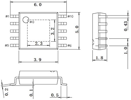
Note: the unit marked in the packaging information drawing is mm (mm).


