|
XG836 Datasheet
(Version 2.0: 2018-7-1)
Catalogue
1. DEVICE OVERVIEW
2. FEATURES
3. PIN ASSIGNMENT
3.1 Pin Description
3.2 PAD Assignment
4. FUNCTIONAL BLOCK DIAGRAM
5. MEMORY
5.1 Program Memory
5.2 Data Memory
5.3 Registers
5.4 Register Table
5.5 Registers description
6. SYSTEM CLOCK AND OPTIONS
6.1 Oscillator
6.2 Crystal Oscillator
6.3 Low Frequency Crystal Oscillator
6.4 External RC Oscillator
6.5 Internal RC Oscillator
6.6 External Clock
7. SYSTEM CONTROL AND RESET
7.1 Reset source
8. INTERRUPT
8.1 Interrupt Vector
9. External Interrupt
10. I/O PORTS
11. TIMER0 MODULE
12. SPI
12.1 SPI Function Description
13. TIMER 1
13.1 Overview
13.2 Function Description
14. ANALOG TO DIGITAL CONVERTER(A/D)
15. DIGITAL TO ANALOG CONVERTER(D/A)
16. ASYNCHRONOUS SERIAL I/O -UART
17. ELECTRICAL CHARACTERISTICS
17.1 Absolute Maximum Ratings
17.2 Electrical Characteristics
XG836 is an 8-bit high performance, low cost MCU which bases on RISC architecture. It is easy to use to deal with analog signal, for example, measurement applications with sensor. The XG836 has an embedded 10-bit analog to digital converter (ADC) with 16 channels, two pulse width modulators (PWM) and one 8-bit digital to analog converter (DAC). It also improved some internal characteristics, such as Halt Function, Wake-up Function, Oscillator Selection, and Programmable Frequency Prescaler. So, XG836 is very flexible for use, and just need least extra parts for cutting down the cost. For these advantages and good characteristics, such as Integrated A/D, Integrated D/A, Integrated PWM, low cost, high performance, flexible Input/Output, and low price, XG836 is very suitable for applications such as Sensor signal process, Motor drive, Industry control, Consumed product, and subsystem controller etc.
XG836 uses Reduced Instruction Set, and it has 256 bytes RAM, the user can easily visit the ROM and RAM but no need to change program page. The special function registers have same addressing mode with RAM
XG836 is One-Time Programmable (OTP), and user’s program can be easily and effectively emulated by our emulator. It provides an effective way for users to develop their program.
· High performance, low cost, 8-bit MCU
· Advanced RISC architecture
- 59 instructions – most of the instructions are executed within one single instruction cycle(Fosc/2)
· Peripheral Features
- One 8-bit timer with frequency prescaler
- One 8-bit pulse width comparator with frequency prescaler
- Watch dog with independent oscillator
- One external interrupt
- One Timer with frequency prescaler and interrupt function.
- Embedded crystal and RC oscillator
- Program interfaces and code protection
- Low voltage reset(LVR)
- 15 I/O ports (P6、P7、P9、PA) with wake-up function
- Two channels of PWM
- 10-bit ADC with 15 channels
- 8-bit DAC with one channel
- A set of UART interface
- Two sets of SPI interface
· Special Microcontroller Features
- Power on reset and power off detect
- Embedded, calibrated RC oscillator
- 6 hardware interrupt sources (external and internal)
- 8 levels stack
- Two sleep modes, halt and sleep to get low consumption
- Instructions are 16-bit,can visit all registers, RAM , ROM and no need to change program page
- Table read function
- Direct addressing and indirect addressing
- Bit oriented instructions
· Memory
- 4K * 16bits OTP ROM
- 256 * 8bits RAM
- 128 * 8bits Special function registers
· I/O and package
- 44 universal I/O ports
- There are two more inputs when use internal RC oscillator
· Ambient operating temperature: 0 ~ 70°C
· Operating voltage range: 2.3 ~ 5.5V
· Operating Frequency range
1. Crystal mode: DC~20MHz at 5V, DC~8MHz at 3V,
2. RC oscillator mode: 3~20MHz at 5V, 3~8MHz at 3V,
· Supply current of XG836 at 6MHz, 5V, 25°C
1. Normal Mode:
It depends on the level of the LDO,
when LDO=3volt, the operating current <1.5mA (no load and transition on all I/Os).
2. Sleep Mode:
< 4.5uA, when LDO on
< 1.5uA, when LDO off
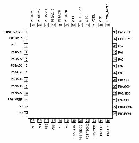
Figure 3.1 Pin assignment
|
Pin name
|
Pin number
|
I/O
type
|
Buffer type
|
Function
|
|
P50
P51/AD1
P51
AD1
P52/AD2
P52
AD2
P53/AD3
P53
AD3
P54/AD4
P54
AD4
P55/AD5
P55
AD5
P56/AD6
P56
AD6
P57/AD7
P57/
AD7
|
3
4
5
6
7
8
9
10
|
I/O
I/O
I
I/O
I
I/O
I
I/O
I
I/O
I
I/O
I
I/O
I
|
TTL
TTL
TTL
TTL
TTL
TTL
TTL
TTL
|
P5 is general purpose bi-directional I/O port, can be pulled high by software
Digital I/O pin, or CS pin when program OTP
Digital I/O pin, or DIO1 pin when program OTP
Analog input 1
Digital I/O pin, or DIO2 pin when program OTP
Analog input 2
Digital I/O pin, or SCK pin when program OTP
Analog input 3
Digital I/O pin
Analog input 4
Digital I/O pin
Analog input 5
Digital I/O pin
Analog input 6
Digital I/O pin
Analog input 7
|
|
P60
P61
P62/SDI2
P62
SDI2
P63/SDO2
P63
SDO2
P64/SCK2
P64
SCK2
P65/SS2
P65
SS2
P66/TX
P66
TX
P67/RX
P67
RX
|
18
19
20
21
22
23
24
25
|
I/O
I/O
I/O
I
I/O
O
I/O
O
I/O
O
I/O
O
I/O
I
|
TTL
TTL
TTL
TTL
TTL
TTL
TTL
TTL
|
P6 is general purpose bi-directional I/O port, can be pulled high by software,can wake up MCU at low
Digital I/O pin
Digital I/O pin
Digital I/O pin
SPI2 data input
Digital I/O pin
SPI2 data output
Digital I/O pin
SPI2 clock output
Digital I/O pin
SPI2 slave device selection
Digital I/O pin
Serial output
Digital I/O pin
Serial input
|
|
P70/VREF
P70
VREF
P71
P72
P73
CLK/P74/P76
DATA/P75/P77
|
11
12
13
14
15
16
|
I/O
I
I/O
I/O
I/O
|
|
P7 is general purpose bi-directional I/O port
Digital I/O pin
AD reference voltage input, less than 3.6V
Digital I/O pin
Digital I/O pin
Digital I/O pin
P74 is connected with P76
P74 can be pulled high by software, can wake up MCU at low
P76 can be set as open drain by software
P75 is connected with P77
P75 can be pulled high by software, can wake up MCU at low
P77 can be set as open drain by software
|
|
P80/AD8
P80
AD8
P81/AD9
P81
AD9
P82/AD10
P82
AD10
P83/AD11
P83
AD11
P84/AD12
P84
AD12
P85/AD13
P85
AD13
P86/AD14/DAO
P86
AD14
DAO
P87/AD15
P87
AD15
|
45
46
47
48
49
50
1
2
|
I/O
I
I/O
I
I/O
I
I/O
I
I/O
I
I/O
I
I/O
I
O
I/O
I
|
TTL
TTL
TTL
TTL
TTL
TTL
TTL
TTL
|
General purpose bi-directional I/O port, can be pulled high by software
Digital I/O pin
Analog input 8
Digital I/O pin
Analog input 9
Digital I/O pin
Analog input 10
Digital I/O pin
Analog input 11
Digital I/O pin
Analog input 12
Digital I/O pin
Analog input 13
Digital I/O pin
Analog input 14
Analog output
Digital I/O pin
Analog input 15
|
|
P90/PWM1
P90
PWM1
P91/PWM2
P91
PWM2
P92/SDI
P92
SDI
P93/SDO
P93
SDO
P94/SCK
P94
SCK
P95/SS
P95
SS
P96
P97
|
26
27
28
29
30
31
32
33
|
I/O
O
I/O
O
I/O
I
I/O
O
I/O
O
I/O
O
I/O
I/O
|
TTL
TTL
TTL
TTL
TTL
TTL
TTL
TTL
|
General purpose bi-directional I/O port, can be pulled high by software
Digital I/O pin, can wake up MCU at low
PWM1 output
Digital I/O pin, can wake up MCU at low
PWM2 output
Digital I/O pin,
SPI data input
Digital I/O pin,
SPI data output
Digital I/O pin,
SPI clock output
Digital I/O pin,
SPI slave device selection
Digital I/O pin,
Digital I/O pin,
|
|
PA0
PA1
PA2
PA3/EINT
EINT
PA3
PA4/VPP
PA4
VPP
PA5/ RESET
RESET
PA5
OSCI
OSCO / PA7
OSCO
PA7
|
34
35
36
37
38
39
42
43
|
I/O
I/O
I/O
I
I/O
I/O
I
I
O
I
|
ST
ST
ST
ST
ST
ST
|
General purpose bi-directional I/O port
Digital I/O pin, can be pulled low by software
Digital I/O pin, can be pulled low by software
Digital I/O pin, can be pulled low by software
External interrupt, internal pull-high, select as EINT when program
Digital I/O pin, can be pulled high by software
Digital I/O pin, can be pulled high by software
PA4 is VPP when Program OTP, input 7.3V voltage
Program pin, external reset, internal pull-high, select as RESET when program
Digital I/O pin, can be pulled high by software
Oscillator input, select as OSCI when program
Oscillator output, select as OSCO when program
Digital input, input voltage must less than 3.6V
|
|
VDD
|
40
|
P
|
|
Power supply, program pin
|
|
VDDL
|
41
|
P
|
|
IC kernel voltage output, program pin
|
|
VSS
|
17,44
|
P
|
|
Power ground, program pin
|
Note: I = Input O = Output I/O = Input/Output P = Power
- = not use TTL = TTL Input ST = Schmitt Input
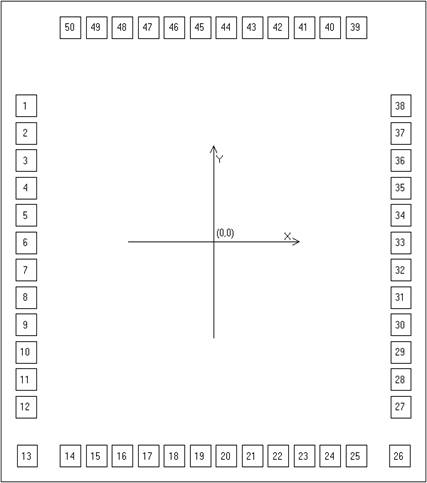
Figure 3.2 Pad Assignment
Unit:μm Note: the underlay must be connected to GND
|
NO.
|
PAD NAME
|
|
NO.
|
PAD NAME
|
|
1
|
P86/AD14/DAO
|
26
|
P90/PWM1
|
|
2
|
P87/AD15
|
27
|
P91/PWM2
|
|
3
|
P50
|
28
|
P92/SDI
|
|
4
|
P51/AD1
|
29
|
P93/SDO
|
|
5
|
P52/AD2
|
30
|
P94/SCK
|
|
6
|
P53/AD3
|
31
|
P95/SS
|
|
7
|
P54/AD4
|
32
|
P96
|
|
8
|
P55/AD5
|
33
|
P97
|
|
9
|
P56/AD6
|
34
|
PA0
|
|
10
|
P57/AD7
|
35
|
PA1
|
|
11
|
P70/VREF
|
36
|
PA2
|
|
12
|
P71
|
37
|
PA3/EINT
|
|
13
|
P72
|
38
|
PA4/VPP
|
|
14
|
P73
|
39
|
PA5/RESET
|
|
15
|
CLK/P74/P76
|
40
|
VDD
|
|
16
|
DATA/P75/P77
|
41
|
VDDL
|
|
17
|
VSS
|
42
|
OSCI
|
|
18
|
P60
|
43
|
PA7/OSCO
|
|
19
|
P61
|
44
|
VSS
|
|
20
|
P62/SDI2
|
45
|
P80/AD8
|
|
21
|
P63/SDO2
|
46
|
P81/AD9
|
|
22
|
P64/SCK2
|
47
|
P82/AD10
|
|
23
|
P65/SS2
|
|
48
|
P83/AD11
|
|
24
|
P66/TX
|
|
49
|
P84/AD12
|
|
25
|
P67/RX
|
50
|
P85/AD13
|
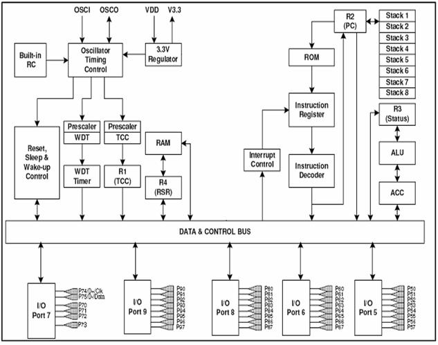
Figure 4.1 Functional Blocks
online document:
https://www.xinga.com/xg/doc/XG836/index.htm
|


 R&D")
 US$2.00 (€1.50)
 US$3.99 (€2.99)
 US$3.99 (€2.99)
 R&D") US$1.00 (€0.75)
US$1.00 (€0.75)